Sharp ER-A850 (serv.man2) Service Manual ▷ View online
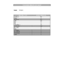
Interface timing table
Item
Symbol
Rating
Unit
Min.
Typ.
Max.
Frame frequency
T
FRM
(Note 1)
8.0
16.9
ms
Clock frequency
T
CP2
152
ns
HIGH level clock width
t
CWH
65
ns
LOW level clock width
t
CWL
65
ns
HIGH level latch clock width
t
LWH
70
ns
Data setup time
t
SU
50
ns
Data hold time
t
H
40
ns
Scan start signal setup time
t
SSU
100
ns
Scan start signal hold time
t
SH
100
ns
Clock allowance time from
CP2
CP2
↓
to CP1
↑
t
S21
0
ns
Clock allowance time from
CP1
CP1
↓
to CP2
↑
t
S12
0
ns
Clock rising/falling time
tr, tf
(Note 2)
trf
ns
(Note 1) The frame frequency (min. 8ms, max q25Hz) is specified
only for the operations.
(Note2)
When CP2 is driven at high speeds, trf is determined by t
CT
in the following formula:
When t
When t
CT
= (T
cp2
– t
CWH
– t
CWL
)/2
u
50, trf = 50
When t
CT
= (T
cp2
– t
CWH
– t
CWL
)/2 < 50, trf = tCT
5. Unit drive procedure
1) Circuit composition
See Fig. 9 on the next page.
2) Screen composition
The display (640
×
480 dot) of this unit is divided into two sections
(the upper half and the lower half) to reduce duty number and provide
high contrast. Each half (640
high contrast. Each half (640
×
240 dot) is driven by 1/240 duty.
3) Input data and control signals
The LCD driver is an 80 bit LSI which is composed of the soft register,
and latch circuit, and the LCD drive circuit.
and latch circuit, and the LCD drive circuit.
Input data are sequentially transmitted from the upper left of each
screen by one line (640 dot) together with clock pulse CP2 through he
shift register as the 4 bit parallel data.
When one line data (= 640 dot data) are inputted, they are latched as
parallel data for 640 signal electrodes at falling edge of latch signal
CP1. The drive signals corresponding to 640 signal electrodes of the
LCD panel are sent to the signal electrodes.
At that time, the scan start signal S inputted to the scan signal drive
circuit is transmitted to the first line to display the signal data in the
first line of each screen in combination with the voltage applied to the
signal electrode.
While the first line data is displayed, the second line data is inputted.
When 640 dot data are transmitted, they are latched at falling edge of
CP1, changing the display to the second line.
As stated above, data inputs are repeated from the top to the bottom
until the 240th line to complete one screen (1 frame). Then the first
line data is inputted again. The scan start signal drives the horizontal
electrodes.
until the 240th line to complete one screen (1 frame). Then the first
line data is inputted again. The scan start signal drives the horizontal
electrodes.
If a DC voltage is applied to the LCD panel, the LCD in the panel is
deteriorated by chemical change. Therefore the drive voltage must be
AC in order to prevent against generation of a DC voltage. This is
performed by the drive waveform AC signal generation circuit.
deteriorated by chemical change. Therefore the drive voltage must be
AC in order to prevent against generation of a DC voltage. This is
performed by the drive waveform AC signal generation circuit.
Fig. 9 Circuit composition block diagram
As the feature of the CMOS driver LSI, the power consumption of the
unit increases as CP2 clock frequency increases. Therefore, the
driver LSI is provided with four shift registers which reduce CP2 clock
data transmitting speed and transmit the 4 bit parallel data.
unit increases as CP2 clock frequency increases. Therefore, the
driver LSI is provided with four shift registers which reduce CP2 clock
data transmitting speed and transmit the 4 bit parallel data.
The LSI reduces the power consumption of the unit. In this circuit
configuration, 4 bit display data are inputted from the data input pin of
DU0
configuration, 4 bit display data are inputted from the data input pin of
DU0
∼
3 (upper half screen) and DL0
∼
3 (lower half screen). In
addition, the LCD unit is provided with the data input bus line system
which reduces the power consumption.
which reduces the power consumption.
This system allows the LSI data input to function only when proper
data are sent.
data are sent.
Data input of the signal electrodes of the upper and lower screens
and the driver LSI chip select are shown below:
and the driver LSI chip select are shown below:
The driver LSI at the left end on the screen is first selected. When 80
dot data (20CP2) are supplied, the right adjacent driver LSI is se-
lected.
This process is repeated sequentially until the data are sent to the LSI
at the right end of the screen.
dot data (20CP2) are supplied, the right adjacent driver LSI is se-
lected.
This process is repeated sequentially until the data are sent to the LSI
at the right end of the screen.
This process occurs simultaneously at the signal electrode drive LSI
in the upper and the lower screens.
As stated above, data input of the upper and the lower screens are
sent through 4 bit bus line sequentially.
in the upper and the lower screens.
As stated above, data input of the upper and the lower screens are
sent through 4 bit bus line sequentially.
Since this graphic display unit does not include a refresh RAM, the
above data and timing pulse must be inputted in a still screen also.
above data and timing pulse must be inputted in a still screen also.
Control
LSI
RAM
C
P
U
P
U
DL0~DL3
S
CP1
CP2
DISP
DU0~DU3
SEG Drivers (Upper)
SEG Drivers (Lower)
V
DD
, V
SS
, V
EE
*2 BG
*1 MG: M GENERATOR CIRCUIT
*2 BG: BIAS GENERATOR CIRCUIT
*2 BG: BIAS GENERATOR CIRCUIT
CO
M
D
ri
v
e
rs
640 X 480 LCD panel
*1 MG
M
Inverter
CCFT
B/L
– 82 –
6. Optical characteristics
The specifications in the table below are the values when the LCD
drive voltage is at the value which makes the contrast maximum in the
vertical direction (
drive voltage is at the value which makes the contrast maximum in the
vertical direction (
θ
x =
θ
y = 0°C).
(Ta = 25°C) V
DD
=5 V, V
DD
– V
EE
= V
MAX.
Item
Symbol
Conditions
Min.
Standard
Max.
Unit
Remark
View angle
range
range
θ
x
Co >
4.0
θ
y = 0°
–25
—
25
Degree
Note 1
θ
y
θ
x = 0°
–10
—
20
Degree
Contrast ratio
Co
θ
x =
θ
y = 0°
10
18
—
Note 2
Re-
sponse
speed
sponse
speed
Rising
τ
r
θ
x =
θ
y = 0°
—
80
130
ms
Note 3
Falling
τ
d
θ
x =
θ
y = 0°
—
70
120
ms
[Note 1]
The view angle is defined as shown in Fig. 4.
[Note 2]
Contrast ratio is defined as shown below:
Co =
Full dot
White
brightness
at Vmax
Full dot Dark
brightness
at Vmax
Vmax is defined in Fig. 6.
[Note 3]
In Fig. 8 optical characteristics measurement method, when
select or non-select signal is given by the dot to be meas-
ured, the response characteristics of the light receiving sec-
tion output value is measured from Fig. 7.
select or non-select signal is given by the dot to be meas-
ured, the response characteristics of the light receiving sec-
tion output value is measured from Fig. 7.
Fig. 4 Definition of view angle
Fig. 5 Optical characteristics measurement method
I
Fig. 6 Definition of Vmax
Fig. 7 Optical characteristics measurement method
II
Fig. 8 Definition of response time
Θ
Θ
Θ
+ y
Θ
+ y
Θ
- y
- x
+ x
Θ
- y
Θ
Θ
Θ
+ y
- x
+ x
Θ
- y
Θ
- x
Θ
+ x
Measuring
Field : 2 ˚
Field : 2 ˚
Θ
+ x
TOPCON BM-7
normal
Θ
- y
Θ
+ y
Θ
- x
Θ
+ y
Θ
- x
Measuring sport size: 10mm
Θ
x: Horizontal angle of the visual angle surface to the vertical suface
Θ
y: Vertical angle of the visual angle surface to the vertical suface
Comax
Vmax
VDD-VEE [V]
Co
n
tra
s
t
Voltage
Θ
TEKTRONIX
TYPE549
Storage
oscilloscope
TYPE549
Storage
oscilloscope
(Response measurement)
Memory
scope
scope
Light receiving element
Lens
Measurement spot size:
∅
0.2mm
Visual sensitivity correction filter
LCD panel
Porlarizing plate
Light source
100%
90
%
1/240 Duty
rr
rd
10
%
[Drive waveform]
Noon-select time
Select time
Non-select time
[Response waveform]
L
igh
t r
e
c
e
iv
ing s
e
c
ti
on
out
p
u
t
rr: Rising time
rd: Falling time
rd: Falling time
– 83 –
7. Backlight characteristics
The backlight specifications are under the following conditions.
1) Rating (Note)
Item
Min.
Standard
Max.
Unit
Brightness
40
65
—
cd/m
2
2) Lamp: FLE-30164C(FA)B-NS115 1 pc.
2-1. Rating (1 pc.)
Item
No conductors
around
Max.
allowance
Circuit voltage
(VS) 1000 V Min.
1500 V
Discharge lamp current
(IL) 5 mA Typ.
7 mA
*
Power consumption
(P) 1.7 W
—
Discharge lamp voltage
(VL) 340 V
—
Brightness
(B) 27000 cd/m
2
Typ.
—
*
The CCFT backlight heat may deteriorate the display quality. The
advisable tube current is, therefore, 5mA or less.
advisable tube current is, therefore, 5mA or less.
2-2 Life time
10,000 hours at rated current 5mA.
However, the following invertor conditions must be satisfied.
However, the following invertor conditions must be satisfied.
•
Positive waveforms and negative waveforms are symmetrical to
each other. No spike waveforms. Must be sine waveforms.
each other. No spike waveforms. Must be sine waveforms.
•
The secondary generation voltage is 1000V or above.
The life is determined when one or two of the following items is or are
satisfied. (25°C
satisfied. (25°C
±
5°C)
a) The discharge start voltage reaches 10.8V.
b) The illumination or light quantity (radiating illumination) reaches
50% of the initial value.
Note: The rating value is the average brightness of five measurement
points (1
∼
5) in the effective display area shown in Fig. 11.
Fig. 11 Measurement point (1
∼
5)
8. Unit handling
8-1. Unit installing angle
The unit has the view angle characteristics as shown in Fig. 12.
θ
y
MIN.
< View angle range <
θ
y
MAX.
(For the values of
θ
y
MIN.
and
θ
y
MAX.
, refer to Fig. 12.)
Fig. 12 Dot matrix LCD view angle
8-2. Unit installation
Install the unit following the precautions in 8-3 without applying unnec-
essary load to the LCD cells and the LSIs. (Be careful not to warp or
twist them.)
essary load to the LCD cells and the LSIs. (Be careful not to warp or
twist them.)
8-3. Note for installation
(1) The surface of polarizing plate is susceptible to damage. Be care-
ful to handle it.
(2) When the LCD panel surface is dirtied, clean it with cotton or soft
cloth.
(3) If water drop is attached for a long time, it may cause stain or
discoloration. Remove it immediately.
(4) Be careful to handle the LCD panel (glass). Be careful not to drop
it or hit with a hard material.
(5) This unit uses the COMS LSI. Be careful to static electricity, and
provide human body grounding.
8-4. Others
(1) Do not leave the unit under the direct sunlight and under strong
ultraviolet rays for a long time.
(2) The internal liquid crystal may be solidified to break cells under the
temperature below the rated storage temperature. Under the tem-
perature above the rated storage temperature, the liquid crystal
may be liquified not to return. Be sure to store it under normal
temperature, normal humidity, and dark place.
perature above the rated storage temperature, the liquid crystal
may be liquified not to return. Be sure to store it under normal
temperature, normal humidity, and dark place.
(3) If the LCD is removed from the unit, contact failure may be
caused. Do not disassemble it.
9. Lot No.
The lot No. is as shown below:
(Example)
(Example)
94
A
00001
( )
Manufacturing factory (Alphabet)
Serial No. (Missing No. exits.)
Month of production (A=January,
B=February, ... L=December)
B=February, ... L=December)
Year of production
dot
1
2
3
4
5
160
320
480dot
120
240
360
Effective display area
-
Θ
y
View angle direction +
Θ
y
Θ
y=0˚ (Normal direction)
(Panel surface)
– 84 –
Touch panel for ER-A880
Note for handling
•
The transparency of the touch panel should be vitally important. Do
not put finger prints or water print on the surface. Use clean finger
such or gloves and masks.
not put finger prints or water print on the surface. Use clean finger
such or gloves and masks.
•
For handling, do not hold the transparent are, and do not hold the
heat seal connector section to assure reliability.
heat seal connector section to assure reliability.
•
Do not overlay touch panels. The edge may damage the surface.
•
Do not put a heavy thing on the touch panel.
•
Do not apply a strong shock, and do not drop it.
•
When attaching the protection film again, carefully check for no
dirt. If there is any dirt, it is transferred.
dirt. If there is any dirt, it is transferred.
•
To clean dirt on the surface, use dry, soft cloth or a cloth immersed
in ethyl alcohol.
in ethyl alcohol.
•
Check that the housing does not give stress to the touch panel.
•
Be careful not to touch the touch panel with tools.
•
The heat seal section is easily disconnected. Be careful not to give
a stress to the heat seal section when installing.
a stress to the heat seal section when installing.
•
The touch panel is provided with an air groove to make the exter-
nal and the internal air pressure equal to each other. If water or oil
is put around the air groove, it may penetrate inside. Be careful to
keep the air groove away from water and oil.
nal and the internal air pressure equal to each other. If water or oil
is put around the air groove, it may penetrate inside. Be careful to
keep the air groove away from water and oil.
•
Input is performed with fingers. Do not use a hard thing for input-
ting.
ting.
KKR0~KKR10 KST0~KST24
KKR0 KKR1
KKR10
KST0
KST1
KST1
KST24
2.11±0.17mm
Upper electrode: R x 2film
Lower electrode: Glass
– 85 –

