Sharp LC-65XS1E (serv.man5) Service Manual ▷ View online
LC-52XS1E/RU/LC-65XS1E/RU
5 – 13
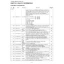
Pin No.
Pin Name
I/O
Pin Function
70, 71
TA1+, TA1-
O
The 1st Link.
The 1st pixel output data when Dual-Link.
The 1st pixel output data when Dual-Link.
68, 69
TB1+, TB1-
64, 65
TC1+, TC1-
58, 59
TD1+, TD1-
56, 57
TE1+, TE1-
62, 63
TCLK1+, TCLK1-
O
LVDS Clock Out for 1st and 2nd Link.
52, 53
TA2+, TA2-
O
The 2nd Link.
These pins are disabled when Single Link.
These pins are disabled when Single Link.
50, 51
TB2+, TB2-
46, 47
TC2+, TC2-
40, 41
TD2+, TD2-
38, 39
TE2+, TE2-
44, 45
TCLK2+, TCLK2-
O
Additional LVDS Clock Out. Identical to TCLK1+,-. No connect if not used.
87 - 84,
81 - 76
R19 ~R10
I
The 1st Pixel Data Inputs.
R1 [9 : 0]
R1 [9 : 0]
99 - 95,
92 - 88
G19 ~G10
G1 [9 :0]
112 -110,
108 -106,
103 - 100
103 - 100
B19 ~B10
B1 [9 :0]
124 - 115
R29 ~R20
I
The 2nd Pixel Data Inputs.
R2 [9 : 0]
R2 [9 : 0]
136 - 127
G29 ~G20
G2 [9 : 0]
6, 5, 2, 1,
144 - 139
144 - 139
B29 ~B20
B2 [9 : 0]
17, 18
CONT11,CONT12
I
CONTROL Data Inputs.
19, 20
CONT21,CONT22
9
DE
I
Data Enable Input.
8
VSYNC
I
Vsync Input.
7
HSYNC
I
Hsync Input.
15
CLKIN
I
Clock Input.
21
R/F
I
Input Clock Triggering Edge Select.
H: Rising edge, L: Falling edge
H: Rising edge, L: Falling edge
22
RS
I
The use of these multi-function depends on input voltage of RS pin.
24
MAP
I
LVDS mapping table select.
H: Mapping Mode1
L: Mapping Mode2
H: Mapping Mode1
L: Mapping Mode2
25, 26
MODE1, MODE0
I
Pixel Data Mode.
Input voltage
of RS pin
of RS pin
VCC
0.6~1.4V
GND
LVDS output
Swing Control
Swing Control
Normal Swing
VOD=350mV(typ)
VOD=350mV(typ)
Reduced Swing
VOD=200mV(typ)
VOD=200mV(typ)
TTL/CMOS Input
VIH/VIL Control for
Small Swing Input
VIH/VIL Control for
Small Swing Input
VIH/VIL is fixed
Support Small Swing Input
VIH/VIL depends on
input voltage of RS pin
See VIH/VIL Spec
VIH/VIL depends on
input voltage of RS pin
See VIH/VIL Spec
VIH/VIL is fixed
MODE 1
MODE 2
MODE
L
L
H
L
L
H
H
H
Dual Link (Dual-in/Dual-out)
Dual Link (Single-in/Dual-out)
Single Link (Dual-in/Single-out)
Single Link (Single-in/Single-out)
LC-52XS1E/RU/LC-65XS1E/RU
5 – 14
19.IC7002 (RH-iXC331WJQZQ)
This is a monitor microprocessor, which receives the remote control light, controls the CEC signal, detects the keys, and detects the OPC. It also
detects the errors relating to the power supply within the IF PWB and controls the power supply of the monitor.
detects the errors relating to the power supply within the IF PWB and controls the power supply of the monitor.
20.IC7006 (VHiBR24L04F-1Y)
This is an EEPROM, in which the portion of the data processed by IC7002 is stored.
21.IC5802 (VHiLTC1154+-1Y)
This is a power supply IC, which supplies 5V for the optional wireless transmission unit. It also detects short circuits and has the thermal shutdown
function.
function.
22.IC5901 (VHiBD9045FV-1Y)
This is a DC/DC converter, which inputs 15V from the power supply unit and generates 5V and 3.3V used within the IF PWB.
2ch DC/DC Converter
27
MODE2
I
Distribution, DDR function enable.
The use of these multi-function depends on the setting of MODE<1:0>.
MODE<1:0>=HH(Single-in/Single-out Mode)
H: Distribution function enable.
L: Distribution function disable.
MODE<1:0>=HL(Single-in/Single-out Mode)
H: DDR (Double Edge input) function enable.
L: DDR (Double Edge input) function disable.
30
/PDWN
I
H: Normal operation,
L: Power down (all outputs are Hi-Z)
L: Power down (all outputs are Hi-Z)
31
PRBS
I
PRBS generator is active when MODE <1:0> = LL (Dual-in/Dual-out mode)
H: PRBS generator is enable. Pattern is PRBS-23.
L: Normal Operation
H: PRBS generator is enable. Pattern is PRBS-23.
L: Normal Operation
10, 11, 12, 16,
28, 32
Reserved
I
Must be tied to GND.
23
Reserved
I
Must be Open.
29, 33, 109
N/C
Must be Open.
3, 13, 82, 93,
104, 113, 125,
137
VCC
-
Power Supply Pins for TTL inputs, output and digital circuitry.
4, 14, 83, 94,
105, 114, 126,
138
GND
-
Ground Pins for TTL inputs, outputs and digital circuitry.
43, 49, 55, 61,
67
LVCC
-
Power Supply Pins for LVDS Outputs.
37, 42, 48, 54,
60, 66, 72
LGND
-
Ground Pins for LVDS Outputs.
35, 74
PVCC
-
Power Supply for PLL circuitry.
34, 36, 73, 75
PGND
-
Ground Pin for PLL circuitry.
Pin No.
Pin Name
I/O
Pin Function
1
OUTL2
O
Low side FET gate drive terminal 2
2
DGND2
-
Low side FET source terminal 2
3
SW2
I
High side FET source terminal 2
4
OUTH2
O
High side FET gate drive terminal 2
5
BOOT2
-
OUTH2 driver power supply terminal
6
CL2
I
Over-current detection setting terminal 2
7
N.C.
-
No Connection
8
VREG5
-
The REG output for FET drive
9
CL1
I
Over-current detection setting terminal 1
10
BOOT1
-
OUTH1 driver power supply terminal
11
OUTH1
O
High Side FET gate drive terminal 1
12
SW1
I
High Side FET source terminal 1
13
DGND1
-
Low side FET source terminal 1
14
OUTL1
O
Low side FET gate drive terminal 1
15
GND
-
Ground terminal
16
TM1
-
Output 1 OCP and an OVP timer latch setting terminal
17
SS1
-
Soft starting time setting terminal 1
Pin No.
Pin Name
I/O
Pin Function
LC-52XS1E/RU/LC-65XS1E/RU
5 – 15
23.IC5902 (VHiBD9045FV-1Y)
This is a DC/DC converter, which inputs 15V from the power supply unit and generates 1.2V and 1.8V used within the IF PWB.
18
COMP1
O
Error amplifier output 1
19
FB1
I
Error amplifier input 1
20
EN1
I
Output 1 ON/OFF terminal
21
VCC
-
Input power supply terminal
22
EN2
I
Output 2 ON/OFF terminal
23
VREG3
-
The REG output for standard power supplies
24
RT
-
Oscillation frequency setting terminal
25
FB2
I
Error amplifier input 2
26
COMP2
O
Error amplifier output 2
27
SS2
-
Soft starting time setting terminal 2
28
TM2
-
Output 2 OCP and an OVP timer latch setting terminal
Pin No.
Pin Name
I/O
Pin Function

