Sharp LC-37AD1E (serv.man10) Service Manual ▷ View online
52
52-1
52-2
LC-37AD1E
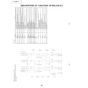
DESCRIPTION OF FUNCTION OF MAJOR ICs
Ë
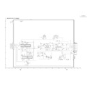
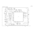
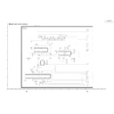
VHISM5301AS-1Y(ASSY:FL810)
3ch output video buffer with a built-in high band filter.
»
Block Diagram
Pin No
.
P
in Name
I/O
Pin Function
»
Pin Function
1
GINA/UINA
I
Analog GINA or a UINA signal input terminal. A synchronized signal is inputted
from a SYNCIN terminal.
2
GSG1
I
The terminal for a GOUT/UOUT output buffer gain setup.
3
GINB/UINB
I
Analog GINB or a UINB signal input terminal. A synchronized signal is inputted
from a SYNCIN terminal.
4
N
C
—
Not connected
5
BINA/VINA
I
Analog BINA or a VINA signal input terminal. A synchronized signal is inputted
from a SYNCIN terminal.
6
G
SB1
I
The terminal for a BOUT/VOUT output buffer gain setup.
7
BINB/VINB
I
Analog BINB or a VINB signal input terminal. A synchronized signal is inputted
from a SYNCIN terminal.
8
N
C
—
Not connected
9
DISABLE
I
Power save function. Pull down resistance built-in.
L : Enable
H : Disable(output terminal (FROUT/YOUT, GOUT/UOUT and BOUT/VOUT are
high impedance.)
10
GND3
—
Analog GND terminal.
11
BOUT/VOUT
O
B/V signal output terminal
12
VCC3
—
A
nalog 5V power supply terminal.
13
GND2
—
Analog GND terminal.
14
GOUT/UOUT
O
G/U signal output terminal
15
VCC2
—
A
nalog 5V power supply terminal.
16
GND1
—
Analog GND terminal.
17
ROUT/YOUT
O
R/Y signal output terminal
18
VCC1
—
A
nalog 5V power supply terminal.
19
GND4
—
Analog GND terminal.
20
RFC
I
L.P.F.(Low path filter) The resistance connection terminal for a cutoff frequency
setup.
21
VFC
I
L.P.F.(Low path filter) The resistance connection terminal for a cutoff frequency
setup.
22
MUXSEL
I
Input terminal selection signal. Pull down resistance built-in.
L : XINA terminal side is chosen.
H : YINB terminal side is chosen.
23
SYNCIN
I
The external H-sync signal input terminal for filter channels.
Active"H." Pull down resistance built-in.
24
VCC4
—
Analog 5V power supply terminal.
25
RINA/YINA
I
Analog RINA or a YINA signal input terminal. A synchronized signal is inputted
from a SYNCIN terminal.
26
GSR1
I
T
he terminal for a ROUT/YOUT output buffer gain setup.
27
RINB/YINB
I
Analog RINB or a YINB signal input terminal. A synchronized signal is inputted
from a SYNCIN terminal.
28
NC
—
Not connected
53
53-1
53-2
LC-37AD1E
Ë
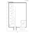
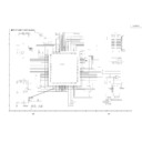
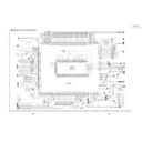
VHITC90A69F-1Y(ASSY:IC401)
3LINE DIGITAL COMB FILTER(NTSC/PAL)
»
Block Diagram
»
Pin Function
Pin No
.
P
in Name
I/O
Pin Function
1
BIAS
—
Bias for ADC
2
VRT
—
D range upper bias for ADC
3
VDD1
—
Power supply for ADC and DAC (analog system)
4
TESTI1
I
Test input
5
VSS2
—
GND for ADC (analog system)
6
VRB
—
D range lower bias for ADC
7
YCIN
I
Picture signal input
8
TEST
O
Reset control and TEST control at the time of shipment
9
K
ILLER
I
Y/C separation and vertical enhancer-off control
10
TESTI2
I
Test input
11
VDD3
—
Power supply for logic (digital system)
12
VSS3
—
GND for Logic and DRAM (digital system)
13
VDD2
—
Power supply for DRAM (digital system)
14
TESTI3
I
Test input
15
SCL
I
Clock input of IIC BUS
16
SDA
I
Data input of IIC BUS
17
MODE1
O
MODE1 output
18
TESTOUT
I
Test input
19
FSC
I
C
lock input
20
VDD4
—
Power supply for PLL (analog system)
21
VSS4
—
GND for PLL (analog system)
22
FIL
I
VCO control
23
PD
O
PLL detection output
24
VB2
—
Bias 2 for DAC
25
YOUT
O
Luminosity signal output
26
VSS1
—
GND for DAC (analog system)
27
COUT
O
Color signal output
28
VB1
—
Bias 1 for DAC
54
54-1
54-2
LC-37AD1E
Ë
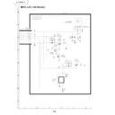
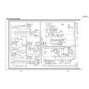
VHITA1318AF1EY (ASSY:IC604)
Synchronous processing for TV component signals, frequency measurement
»
Block Diagram
Pin No
.
P
in Name
I/O
Pin Function
»
Pin Function
1
H
D2-IN
I
Input the horizontal synchronizing signal.
It's polarity corresponds to both positive and negative.
Input from this pin does not be synchronized internally.
2
VD2-IN
I
Input the vertical synchronizing signal.
It's polarity corresponds to both positive and negative.
Input from this pin does not be synchronized internally.
3
HD1-IN
I
Input the horizontal synchronizing signal.
It's polarity corresponds to both positive and negative.
Input from this pin does not be synchronized internally.
4
VD1-IN
I
Input the vertical synchronizing signal.
It's polarity corresponds to both positive and negative.
Input from this pin does not be synchronized internally.
5
A
NALOG GND
—
The GND pin for analog circuit block.
6N
.C
—
It is a blank terminal. Please connect with GND.
7
AFC FILTER
—
Connect the filter for horizontal AFC. The frequency of the horizontal output is
varied by the volyage at this pin.
8N
.C
—
It is a blank terminal. Please connect with GND.
9
HVCO
—
Connect the ceramic oscillator for horizontal oscillator.
10
N.C
—
It is a blank terminal. Please connect with GND.
11
VCC
—
The VCC pin.(9.0V)
12
DAC2(H/C.
O
DAC2 output pin. When TEST mode, HD or composite sync signal to frequency
SYNC output)
counter circuit is output.
13
VD3-IN
I
Input the vertical synchronizing signal.
It's polarity corresponds to both positive and negative.
14
HD3-IN
I
Input the horizontal synchronizing signal.
It's polarity corresponds to both positive and negative.
15
CP-OUT
O
C
lamp pulse output pin. CP according to the incoming signal by which
synchronous reproduction is carried out is outputted.
16
HD1-OUT
O
HD output pin. This pin is open-collector system.
HD1/HD2 input signal is outputted from this terminal, without carrying out
synchronous processing.
It's polarity is switched by BUS write function.
17
N.C
—
It is a blank terminal. Please connect with GND.
18
DIGITAL GND
—
The GND pin for digital circuit block.
19
HD2-OUT
O
HD output pin. This pin is open-collector system.
HD1/HD2 input signal is outputted from this terminal, without carrying out
synchronous processing.
It's polarity is switched by BUS write function.
20
N.C
—
It is a blank terminal. Please connect with GND.
21
SDA
I/O
The SDA pin for I2C BUS.
22
SCL
I
The SCL pin for I2C BUS.
23
ADDRESS SW
I
S
lave address switch.
24
SYNC2-IN
I
It is the input of a synchronous separation circuit.
Y signal is inputted through a clamp capacitor.
25
DAC1(V. SYNC
O
DAC1 output pin. When TEST mode, VD or vertical sync signal to frequency
output)
counter circuit is output.
26
SYNC1-IN
I
It is the input of a synchronous separation circuit.
Y signal is inputted through a clamp capacitor.
27
N.C
—
It is a blank terminal. Please connect with GND.
28
VD1-OUT
O
VD output pin. This pin is open-collector system.
VD1/VD2 does not be synchronizing and they are output from this pin.
It's polarity is switched by BUS write function.
29
VD2-OUT
O
VD output pin. This pin is open-collector system.
VD1/VD2 does not be synchronizing and they are output from this pin.
It's polarity is switched by BUS write function.
30
DAC3
O
DAC2 output terminal. This pin is open-collector system. The pulse signal for a
shipment test is outputted at the time of TEST mode.
55
55-1
55-2
LC-37AD1E
Ë
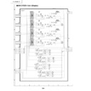
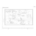
VHITB1274AF1EQ (ASSY:IC801)
VIDEO/CHROMA/SYNC. processor
»
Block Diagram
»
Pin Function
Pin No
.
P
in Name
I/O
Pin Function
1
CVBS1/Y1-IN
I
CVBS1 or a Y1-IN signal is inputted.
2
SYNC-IN
I
Synchronized signal is inputted.
3
CVBS-OUT
O
O
utput terminal of CVBS or a Y+C signal.
4
V
S
O
Counted-down vertical synchronized signal is outputted.
5
COMB Y-IN
I
Y
-signal outputted from comb-filter is inputted.
It opens, when not using it.
6
D-VDD
—
Power supply of a DDS/BUS/V-CD/H-CD block is supplied.
DC5V (standard)"
7
COMB C-IN
I
C-signal outputted from comb-filter is inputted.
It opens, when not using it."
8
D
-GND
—
GND terminal of a DDS/BUS/V-CD/H-CD block.
9
H
S
O
Horizontal synchronized signal which required H-AFC is outputted.
10
SCP
O
Sand Castle Pulse is outputted. A clamp pulse and a horizontal Blanking pulse
are outputted.
11
Yvi-IN
O
Y
-signal for a synchronous input selected by Video-SW is outputted.
12
SYNC-VCC
—
Power supply of a SYNC/HVCO block is supplied.
DC5V (standard)
13
SCL
I
SCL terminal of I2CBUS.
14
SDA
I/O
SDA terminal of I2CBUS.
15
YS3(RGB1-in)
I
S
electe SW of a main signal and RGB1 input signal.
Only when "RGB1-ENB" is set as "enable" by bus setup, the input of YS3
becomes effective.
16
SYNC-GND
—
GND terminal of a SYNC/HVCO block.
17
Cr1-IN
I
Y1-/Cb1/Cr1 signal is inputted.
18
Cb1-IN
I
19
Y1-IN
I
20
CLP-FIL
—
Filter for Y clamp is connected.
21
Y-OUT
O
Y/Cb/Cr signal is outputted.
22
Cb-OUT
O
23
Cr-OUT
O
24
YS1(YVbC2-IN)
I
Selecte SW of a main signal and YCrCb2 input signal.
25
B1-IN
I
RGB1 signal is inputted. This input is selected in YS3 or I2CBUS.
26
G1-IN
I
27
R1-IN
I
28
Y/C-GND
—
GND terminal of Y/C/Text/Video-SW / 1HDL block.
29
Cr2-IN
I
Y2/Cb2/Cr2 signal is inputted. This input is selected in YS1.
It opens, when not using it.
30
Cb2-IN
I
31
Y2-IN
I
32
Y/C-VCC
—
Power supply of Y/C/Text/Video-SW / 1HDL block is supplied.
DC5V (standard)
33
B2-IN
I
RGB2 signal is inputted. This input is selected in YS2.
It opens, when not using it.
34
G2-IN
I
35
R2-IN
I
36
YS2/YM(RGB2-IN)
I
S
electe SW of a main signal and RGB2 input signal.
37
FIL.
—
Connects with a Y/C-VCC terminal.
38
X'TAL
—
16.2MHz X'tal oscillation element is connected.
39
C3-IN
I
Chrominance signal is inputted. It opens, when not using it.
40
APC-FIL
—
Filter for a chrominance demodulater is connected.
41
CVBS3/Y3-IN
I
CVBS3 or Y3 signal is inputted. It opens, when not using it.
42
ADDRESS
I
S
lave address is set up.
43
C2-IN
I
Chrominance signal is inputted. It opens, when not using it.
44
CVBS2/Y2-IN
I
CVBS2 or Y2 signal is inputted. It opens, when not using it.
45
COMB SYS
O
The distinction result of the received color system is outputted from this terminal
and a terminal 46.
46
Fsc-OUT
O
Subcarrier is outputted.
47
AFC-FIL
—
Filter for AFC detection is connected.
48
C1-IN
I
Chrominance signal is inputted. It opens, when not using it.

