Sharp AL-1611 (serv.man15) Service Manual ▷ View online
AL-1611/AL-1622
ELECTRICAL SECTION
13 – 13
199
A2
A2
IN
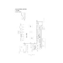
System bus
200
GND
POW
201
VCC
POW
202
A3
A3
IN
System bus
203
A4
A4
IN
System bus
204
A5
A5
IN
System bus
205
VCC
POW
206
A6
A6
IN
System bus
207
A7
A7
IN
System bus
208
GND
POW
209
RSTB
/RESET
IN
System reset
0: Reset
210
GND
POW
211
CLK
CPUCLK
IN
System clock
212
GND
POW
213
D0
D0
BIDIR
System bus
214
D1
D1
BIDIR
System bus
215
D2
D2
BIDIR
System bus
216
GND
POW
217
D3
D3
BIDIR
System bus
218
D4
D4
BIDIR
System bus
219
D5
D5
BIDIR
System bus
220
VCC
POW
221
GND
POW
222
D6
D6
BIDIR
System bus
223
D7
D7
BIDIR
System bus
224
VCC
POW
225
D8
D8
BIDIR
System bus
226
D9
D9
BIDIR
System bus
227
D10
D10
BIDIR
System bus
228
D11
D11
BIDIR
System bus
229
D12
D12
BIDIR
System bus
230
D13
D13
BIDIR
System bus
231
D14
D14
BIDIR
System bus
232
GND
POW
233
D15
D15
BIDIR
System bus
234
PMC1POUT0
SPFDA
OUT
SPF motor phase A drive
H: Drive
235
PMC1POUT1
SPFDB
OUT
SPF motor phase B drive
H: Drive
236
PMC1POUT2
/SPFDA
OUT
SPF motor phase /A drive
H: Drive
237
PMC1POUT3
/SPFDB
OUT
SPF motor phase /B drive
H: Drive
238
DSCLK
DSCLK
ODN
Document size sensor control
239
DSLED0
LED0
OUT
2: Beam document size sensor control
240
VCC
POW
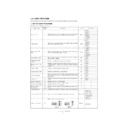
Pin No.
Pin name
Signal name
I/O
Purpose
Descriptions
Pin descriptions) IN: Input pin OUT: Output pin BIDIR: Bi-directional pin ODN: Open drain output pin TR1: 3-state output pin POW: Power pin
AL-1611/AL-1622
ELECTRICAL SECTION
13 – 14
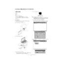
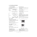
E. RESET CIRCUIT
This circuit detects ON/OFF of power to control start/stop of each circuit. The 5V voltage and WTOVF signal of the main PWB is detected by the reset
IC to generate the reset signal.
When the power voltage reaches the specified level, the circuit operations are started. Before the power voltage falls below the specified level, the cir-
cuit operations are stopped to prevent against malfunctions.
cuit operations are stopped to prevent against malfunctions.
F. MAIN MOTOR DRIVE CIRCUIT
The main motor is driven by the MMD signal from ASIC. While the main motor is rotating, the MMD signal is driven to HIGH and passed through IC35
to the control circuit in the main motor to rotate the main motor. The /MMRDY signal is kept HIGH until the main motor speed reaches the specified
to the control circuit in the main motor to rotate the main motor. The /MMRDY signal is kept HIGH until the main motor speed reaches the specified
rpm, and passed to the CPU.
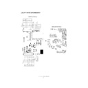
G. MIRROR MOTOR CIRCUIT
The mirror motor is a stepping motor, and it uses the IC29 and the constant current chopper control IC (SLA7027). For control, the CPU outputs the
drive signal to the IC29 to drive the mirror motor with 1-2 phase excitement.
IC3A
IC2
RESET
VSB
VSA
VCC
NJM2103M
74VHC09
1
/RESET
3
2
7
6
6
2
1
3
8
4
NP
C2
VCC
1
C
1
1
C
2
0
.1
C3
CPU
RES
WDTOVF
5
IC1
CPU
CPU
MM
IC31
Driver
Driver
IC32
2
18
4
96
97 /MMRDY#
MMD
14
/MMRDY
/MMD
IC5
ASIC
ASIC
MIRROR
MOTOR
MOTOR
MMCC12
MMCC01
29
31
30
28
IC31
+
IC25
SLA7027MU
+
2200p
ICPN38
24V
/MMA
MMB
MMB
MMA
F6
2.4K
1.0(2W)
/MMB
4
7
/3
5
V
2.4K
2200p
1.0(2W)
4
7
0
p
4
7
0
p
6
2
0
1
00
6
2
0
4
7
K
5
1
0
4
7
K
22
/1
6
V
/MMRMO0
/MMRMO1
VCC
1
2
13
14
17
16
4
5
3
9
15
10
7
8
12
11
18
4
70
71
71
1
2
16
15
MIRMODA
MIRMODB
/MIRMODB
/MIRMODB
/MIRMODA
1
2
3
4
7
5
8
1
6
TDB
TDA
REFB
INA
RSA
INB
INA
INB
REFA
OUTB
VSB
VSA
RSB
OUTA
GA
OUTA
OUTB
GB
AL-1611/AL-1622
ELECTRICAL SECTION
13 – 15
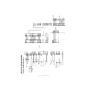
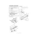
H. TONER SUPPLY MOTOR DRIVE CIRCUIT
The IC31 is the motor control IC, which generates the pseudo AC waveform with the pulse signals (TM, TM-) outputted from ASIC, driving the toner
supply motor.
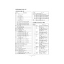
3. CCD PWB
The CCD PWB is provided with the CCD (Charge-Coupled Device), the differential amplifier which amplifies image signals, and the AD convertor
which converts the amplified image signals into digital signals.
The DC power and the pulse supply pins necessary for operating the CCD image sensor are the power source (CD pin), GND (SS pin), shift pulse
(SH pin), transfer pulse (
φ
1 pin), (
φ
2 pin), reset pulse (/RS pin), clamp pulse (/CP pin), and sampling (/SP pin).
interval between inputting two SH signals is called the photo accumulation time.
The signals are transfered to the register, then to the shift register sequentially by transfer pulses
φ
1 and
φ
2 and to the floating capacitor section
where electric signals are voltage-converted. Electric charges from the even number pixel shift register and the odd number pixel shift register are
flowed to the floating capacitor section alternatively.
flowed to the floating capacitor section alternatively.
The /RS signal is the reset signal of the CCD output signal. The CCD output is expressed as electric charges equivalently accumulated in the capac-
itor. Therefore, to take the CCD output data one pixel by one pixel, one output data must be cleared after it is outputted. The /RS signal is used for
that operation.
The /SP pulse signal is the peak hold signal of the signal voltage.
The output signal from the CCD is amplified by about 4.7 times greater in the differential amplifier circuit in the CCD PWB.
Differential amplification is made for the signal output (OS) and the compensation output (DOS).
The amplified CCD signal output is sent to the clamp circuit. In the clamp circuit, the black level is clamped to 2V at the BCLK signal timing by the
analog switch. The clamped voltage is maintained for one line by the coupling capacitor. The clamped analog signal is impedance-converted and
analog switch. The clamped voltage is maintained for one line by the coupling capacitor. The clamped analog signal is impedance-converted and
inputted to the AD convertor.
The analog signal inputted to the AD convertor is converted into 8bit digital data and passed to the PCU PWB.
The machine employs the TCD1501C as the image sensor. The TCD1501C is the reduction type high sensitivity CCD linear sensor of one-output
24V
2
9
1
4
IC27
TA7291S
IN1
IN2
GND
6
7
7
3
8
5
5
OUT1
OUT2
V5
VCC
GND
Vref
47K
47K
+
VCC
1
0µ/
1
6
V
TM
+
IC1 CPU
DTC114EKA
4.7K(1/4W)
76/
PWOFF
PWOFF
10K
1SS133
10K
4.7K(1/4W)
47K(1/4W)
TMD
/TMD
DTC114EKA
1SS133
10 /25V
229
/TM
228
TM
/TM
TM
/PWOFF
IC13
Image
ASIC
Image
ASIC
CCD analog shift register 1
CCD analog shift register 2
Photo diode
12V
Output
Photo diode
Accumulation electrode
Shift electrode
To Shift register
Photo energy

