Sharp AL-1611 (serv.man15) Service Manual ▷ View online
AL-1611/AL-1622
ELECTRICAL SECTION
13 – 1
[13] ELECTRICAL SECTION
1. OUTLINE
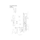
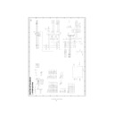
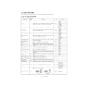
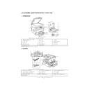
A. BLOCK DIAGRAM
MCU-PWB
CC
D
-PW
B
A
PC-PW
B
S
P
F
-SEN
-PWB
S
P
F
-C
O
N
-PW
B
2nd
C
S
-PWB
HIGH V
O
LT
A
G
E
U
N
IT
PWB
P
O
W
E
R
S
UPP
L
Y
PWB
P
S
-F
A
N
P
S
-S
W
P
olygo
n
-M
otor
M
irror
-M
otor
S
P
F
-M
otor
S
P
F
-C
LH
S
P
F
-R
S
O
L
D
sub
-2
5p
in
S
P
F
-G
S
O
L
S
P
F
-P
S
O
L
L
1
L
2
F
us
e
r-
L
am
p
C
o
p
y
-L
am
p
D
o
w
n
-L
o
a
d
-C
O
N
P
IC
K
UP
S
O
L
1
FEE
D
S
O
L
1
P
IC
K
UP
S
O
L
2
T
o
n
e
r-M
o
tor
M
A
IN
-M
otor
TH
E
R
M
IS
T
E
R
O
P
E
R
A
TI
O
N
P
A
NE
L
E
R
D
H
-O
P-PWB
C
O
P
Y
-O
P-PWB
C
A
SS
1
PP
D
1
D
R
S
1
C
SS
1
C
A
SS
2
PP
D
2
C
A
SS
:C
S
U
N
IT
D
E
T
E
C
T
O
R
C
SS
:P
A
P
E
R
D
E
T
E
C
T
O
R
PP
D
:P
A
P
E
R
P
A
SS
D
E
T
E
C
T
O
R
D
R
S
:D
OO
R
D
E
T
E
C
T
O
R
H
A
N
D
P
IC
K
UP
S
O
L
C
N
1
5
C
N
1
9
P
S
R
O
LL
E
R
S
O
L
C
N
1
8
C
N
1
0
C
N
1
3
C
N
1
2
B
D
-PWB
L
S
U-PWB
C
N
4
C
N
3
1
C
N
6
C
N
5
C
N
11
F
U
SE
R
C
OO
LI
N
G
F
A
N
C
N
2
3
C
N
2
4
D
R
UM
I
N
ITI
A
L
S
W
IT
C
H
C
N
1
6
C
N
2
0
C
N
3
5
C
N
2
C
N
1
S
ID
E
C
O
V
E
R
C
A
SE
TT
E
S
W
IT
C
H
S
W
IT
C
H
C
N
1
4
C
N
22
D
E
V
SENS
O
R
C
N
2
7
C
A
SE
TT
E
P
IC
K
UP
S
O
L
H
A
N
D
P
A
P
E
R
E
MP
T
Y
SENS
O
R
C
A
SE
TT
E
P
A
P
E
R
E
MP
T
Y
SENS
O
R
C
N
3
2
C
N
33
P
A
P
E
R
I
N
SENS
O
R
C
N
2
8
S
C
A
NNE
R
H
P
SENS
O
R
S
C
A
NNE
R
C
O
V
E
R
S
W
IT
C
H
C
N
2
9
C
N
1
7
C
N
2
6
O
N
L
Y
A
L
-1
6
22
O
N
L
Y
A
L
-1
6
22
C
O
P
Y
L
A
MP
U
N
IT
L
A
MP
D
R
IV
E
PWB
L
A
SE
R
S
C
A
N
U
N
IT
CPU
CPU
C
N
3
6
I/
O
E
X
P
A
N
D
A
S
IC
G
R
A
P
HI
C
A
S
IC
C
N
3
8
C
R
UM
U
N
IT
AL-1611/AL-1622
ELECTRICAL SECTION
13 – 2
2. MCU
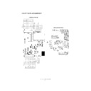
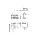
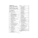
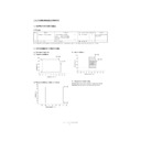
A. BLOCK DIAGRAM (MCU)
B. CPU (HD6412351IF)
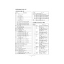
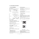
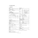
(1) pin/signal table
AL-1622
only
only
CRUM
UNIT
UNIT
Pin No.
Pin name
Signal name
I/O
Function
Purpose
Descriptions
1
/CS1
/CS1
OUT
Area 1 chip select
SRAM chip select
L: Select
2
/CS0
/CS0
OUT
Area 0 chip select
Flash ROM chip select
L: Select
3
VSS
POW
Ground pin
4
VSS
POW
Ground pin
5
VCC
POW
Power pin
6
A0
A0
OUT
Address bus 0
System bus
7
A1
A1
OUT
Address bus 1
System bus
8
A2
A2
OUT
Address bus 2
System bus
9
A3
A3
OUT
Address bus 3
System bus
10
VSS
POW
Ground pin
11
A4
A4
OUT
Address bus 4
System bus
12
A5
A5
OUT
Address bus 5
System bus
13
A6
A6
OUT
Address bus 6
System bus
14
A7
A7
OUT
Address bus 7
System bus
15
A8
A8
OUT
Address bus 8
System bus
16
A9
A9
OUT
Address bus 9
System bus
17
A10
A10
OUT
Address bus 10
System bus
18
A11
A11
OUT
Address bus 11
System bus
19
VSS
POW
Ground pin
20
A12
A12
OUT
Address bus 12
System bus
21
A13
A13
OUT
Address bus 13
System bus
(Pin descriptions) IN: Input pin
OUT: Output pin
BIDIR: Bi-directional pin
ODN: Open drain output pin
TR1: 3-state output pin
POW: Power pin
AL-1611/AL-1622
ELECTRICAL SECTION
13 – 3
22
A14
A14
OUT
Address bus 14
System bus
23
A15
A15
OUT
Address bus 15
System bus
24
A16
A16
OUT
Address bus 16
System bus
25
A17
A17
OUT
Address bus 17
System bus
26
A18
A18
OUT
Address bus 18
System bus
27
A19
A19
OUT
Address bus 19
System bus
28
VSS
POW
Ground pin
29
A20
A20
OUT
Address bus 20
System bus
30
/IRQ5
/SPFCOVER
IN
Interruption request 5
SPF cover sensor interrup-
tion
tion
1: Cover close
31
/IRQ6
/OCCOVER
IN
Interruption request 6
OC cover sensor interrup-
tion
tion
0: Cover close
32
/IRQ7
MHP
IN
Interruption request 7
Mirror home position sensor
interruption
interruption
1: Home position
33
/IRQ3
/SPFPAPER
IN
Interruption request 3
S P F p a p e r p a s s s e n s o r
interruption
interruption
0: Paper presence
34
/IRQ2
/CPUSYNC
IN
Interruption request 2
Horizontal sync signal inter-
ruption
ruption
0: Effective
35
VSS
POW
Ground pin
36
VSS
POW
Ground pin
37
/IRQ1
/FW
IN
Interruption request 1
Zero cross interruption
0: Effective
38
/IRQ0
/LOOPINT
IN
Interruption request 0
Loop interruption
0: Effective
39
VCC
POW
Power pin
40
D0
D0
BIDIR
Data bus 0
System bus
41
D1
D1
BIDIR
Data bus 1
System bus
42
D2
D2
BIDIR
Data bus 2
System bus
43
D3
D3
BIDIR
Data bus 3
System bus
44
VSS
POW
Ground pin
45
D4
D4
BIDIR
Data bus 4
System bus
46
D5
D5
BIDIR
Data bus 5
System bus
47
D6
D6
BIDIR
Data bus 6
System bus
48
D7
D7
BIDIR
Data bus 7
System bus
49
D8
D8
BIDIR
Data bus 8
System bus
50
D9
D9
BIDIR
Data bus 9
System bus
51
D10
D10
BIDIR
Data bus 10
System bus
52
D11
D11
BIDIR
Data bus 11
System bus
53
VSS
POW
Ground pin
54
D12
D12
BIDIR
Data bus 12
System bus
55
D13
D13
BIDIR
Data bus 13
System bus
56
D14
D14
BIDIR
Data bus 14
System bus
57
D15
D15
BIDIR
Data bus 15
System bus
58
VCC
POW
Power pin
59
P30
OUT
General port 30
(Not used)
L: Level fixing output
60
TXD1
TXD1
OUT
SCI channel 1 serial trans-
mission
mission
Service connector
UART serial output
61
P32
SDA
ODN
General port 32
EEPROM control
12CBUS data line
62
RXD1
RXD1
IN
SCI channel 1 serial recep-
tion
tion
Service connector
UART input
63
P34
SCL
ODN
General port 34
EEPROM control
12CBUS clock line
64
P35
/FROMUP
IN
General port 35
Service connector
0: Service mode
65
VSS
POW
Ground pin
66
/DREQ0
/DREQ0
IN
DMAC channel 0 external
request
request
Mirror and SPF motor accel-
eration/reduction control
eration/reduction control
0: Request effective
67
VSS
POW
Ground pin
Pin No.
Pin name
Signal name
I/O
Function
Purpose
Descriptions
(Pin descriptions) IN: Input pin
OUT: Output pin
BIDIR: Bi-directional pin
ODN: Open drain output pin
TR1: 3-state output pin
POW: Power pin
AL-1611/AL-1622
ELECTRICAL SECTION
13 – 4
68
VSS
POW
Ground pin
69
/CS5
OUT
Area 5 chip select
(Not used)
L: Select
70
/DREQ1
/DREQ1
IN
DMAC channel 1 external
request
request
Lifter and separator motor
acceleration/reduction con-
trol
acceleration/reduction con-
trol
0: Request effective
71
P63
POFFR
OUT
General port 63
Power off relay control
H: AC switch OFF
72
P27
/ESPAGE
IN
General port 27
ERDH option page signal
detection
detection
0: Page effective
73
P26
/PCLPAGE
IN
General port 26
PCl operation page signal
detection
detection
0: Page effective
74
P25
/FAXPAGE
IN
General port 25
F A X o p t i o n p a g e s i g n a l
detection
detection
0: Page effective
75
P24
/READY
OUT
General port 24
Machine ready signal
L: Machine ready state
76
P23
/PWOFF
OUT
General port 23
Power off signal
L: Power interruption detect-
ing state
ing state
77
P22
/SCANSP
OUT
General port 22
Scan stop signal
L: Scanning operation inter-
ruption
ruption
78
P21
/SCANST
OUT
General port 21
Scan start signal
L: Scanning operation effec-
tive
tive
79
P20
/PRSTART
OUT
General port 20
Print start signal
L: Printing effective
80
/WDTOVR
OUT
Watch dog timer overflow
System reset
L: System restart
81
/RES
IN
System reset
System reset
0: Power on reset
82
NMI
IN
Non-maskable interruption
request
request
(Not used)
1: Level fixing input
83
/STBY
IN
Stand-by
(Not used)
1: Level fixing input
84
VCC
POW
Power pin
85
XTAL
IN
Oscillation pin
Oscillator (19.6608MHz)
86
EXTAL
OUT
Oscillation pin
Oscillator (19.6608MHz)
87
VSS
POW
Ground pin
88
â
CPUCLK
OUT
System clock
System clock
19.6608MHz clock output
89
VCC
POW
Power pin
90
/AS
/AS
OUT
Address strobe
System bus
L: Address effective
91
/RD
/RD
OUT
Lead strobe
System bus
L: Lead effective
92
/HWR
/HWR
OUT
Highlight enable
System bus
L: Highlight effective
93
/LWR
/LWR
OUT
Row write enable
System bus
L: Row write effective
94
PF2
/TMEN
OUT
General port F2
Toner motor drive control
L: Rotating
95
PF1
PMD
OUT
General port F1
Polygon motor drive control
H: Rotating
96
PF0
MMD
OUT
General port F0
Main motor drive control
H: Rotating
97
P50
/MMRDY
IN
General port 50
Main motor ready signal
0: Rotation stable state
98
P51
/PMRDY
IN
General port 51
Polygon motor ready signal
0: Rotation stable state
99
VSS
POW
Ground pin
100
VSS
POW
Ground pin
101
P52
/PRLINE
OUT
General port 52
Print line signal
L: Printing effective
102
P53
/SCLINE
OUT
General port 53
Scan line signal
L: Scanning operation effec-
tive
tive
103
AVCC
POW
Analog power pin
104
VREF
POW
Analog reference pin
105
AN0
RTH
IN
Analog input 0
Fusing thermistor tempera-
ture detection
ture detection
106
AN1
IN
Analog input 1
(Not used)
107
AN2
IN
Analog input 2
(Not used)
108
AN3
TONER
IN
Analog input 3
Toner sensor
5V: Toner empty
109
AN4
IN
Analog input 4
(Not used)
110
AN5
IN
Analog input 5
(Not used)
111
DA0
DA0
OUT
Analog output 0
CCD reference + side
Pin No.
Pin name
Signal name
I/O
Function
Purpose
Descriptions
(Pin descriptions) IN: Input pin
OUT: Output pin
BIDIR: Bi-directional pin
ODN: Open drain output pin
TR1: 3-state output pin
POW: Power pin

