Sharp LC-19A1E (serv.man5) Service Manual ▷ View online
LC-19A1E-BK/WH
5 – 31
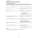
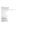
2.19. IC7501 (VHiBD9883FV)
2.19.1 Block Diagram
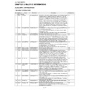
2.19.2 Pin Connections and short description
Pin No.
Pin Name
I/O
Pin Function
1
DUTY
I
Switch terminal of PWM mode and BURST mode.
2
BCT
-
Capacity connecting terminal for setting BURST oscillator frequency.
3
BRT
-
Resistance connecting terminal for setting the charge and discharge current of BCT terminal
4
CT
-
Capacity connecting terminal for setting Oscillator Frequency.
5
RT
-
Resistance connecting terminal for setting the charge and discharge current of CT terminal.
6
SRT
-
Resistance connecting terminal for setting the charge and discharge current of CT terminal.
7
GND
-
Ground.
8
FB
O
Error amplifier output. (FB)
9
IS
I
Error amplifier input 1. (IS)
10
VS
I
Error amplifier input 2. (VS)
11
STB
I
stand-by switch terminal.
12
SCP
-
Capacity connecting terminal for setting SCP timer.
13
SS
O
Capacity connecting terminal for setting soft start.
14
PGND
-
GND terminal of a built-out FET drive circuit.
15
LN
O
The output terminal of a bult-out FET drive circuit. (LN)
16
HN
O
The output terminal of a bult-out FET drive circuit. (HN)
17
SW
O
Low voltage rail terminal for HN output. (Earth)
18
BST
I
Boot-Strap input terminal for HN output.
19
REG
O
The output voltage terminal of an internal regulator circuit.
20
VCC
-
Supply voltage input.

