Sharp LC-19A1E (serv.man5) Service Manual ▷ View online
LC-19A1E-BK/WH
5 – 1
Service Manual
CHAPTER 5.
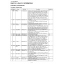
MAJOR IC INFORMATIONS
[1] MAJOR IC INFORMATIONS
1. MAJOR IC INFORMATIONS
No.
Ref No.
Name
Part Code
Description
Drawing No.
[MAIN Section]
1
IC801
DVP-M2
RH-iXB882WJZZQ
DVP-M2 is 1 chip picture signal processing LSI for flat panel displays
corresponding to a multi-format (NATC/PAL/SECAM). A 10-bit A/D
converter is mounted as an analog image input, and it has the input
terminal of one CVBS, Y/C, Y/Pb/Pr, one R/G/B input each, and one
SCART input. In a picture signal processing part, a high definition
image is made by three-dimensional adaptation type Y/C separation
and motion adaptation three-dimensional NR conversion. DVP-M 2S
builds in 64 M bit SDRAM as a buffer memory, the microcomputer for
system control (32/16 bit), 1024 K bytes of flash memory, and the
sound multiplex decoder, and constitutes the system from small num-
ber of parts.
M1
2
IC803
64Kbit-E2PROM
VHiS24CS64A-1Y
The BR24L64F is a 64Kbit-2-wire (I2C bus type) serial EEPROM that
is electrically programmable.
This IC serves to store the adjustment and other data in the adjust-
ment process mode.
The data is given out by commands from the main microprocessor.
is electrically programmable.
This IC serves to store the adjustment and other data in the adjust-
ment process mode.
The data is given out by commands from the main microprocessor.
M1
3
IC2001
RESET
VHiPST8229N-1Y
It used to system reset for sub-micon (IC2002).
M2
4
IC2002
SUBMICON
RH-iXC165WJZZQ
IXC165WJ is the submicrocomputer added in order to compensate
the shortage of control with DVP-M2 (MAIN-MICON). This IC mounts
with the R8C/Tiny series core. It has the capability to execute a com-
mand at high speed, and high-speed operation processing is possible.
Moreover, variegated peripheral equipment, such as a multifunctional
timer, serial interface, and a data flash (1KB * 2 blocks), is built in.
M2
5
IC2003
4Kbit-E2PROM
VHiBR24L04F-1Y
The BR24L04F is a 4Kbit-2-wire (I2C bus type) serial EEPROM that is
electrically programmable.
This IC saves the control data such as un uncontrollable control signal
by MAIN-MICON (it builds in IC801) etc.
The data is given out by commands from the sub microprocessor.
electrically programmable.
This IC saves the control data such as un uncontrollable control signal
by MAIN-MICON (it builds in IC801) etc.
The data is given out by commands from the sub microprocessor.
M2
6
IC2004
Series regulator
VHiPQ1LAX95-1Y
This IC generates B3.3V-regurator.
M2
7
IC702
Series regulator
VHiPQ1LAX95-1Y
This IC generates B9V-regurator.
M9
8
IC9201
RSDS-transmitter RH-iXC209WJZZQ
IXC209WJ (LR38875) is a RSDS transmitter for LCD controllers.
LVDS RGB 8bit data and a clock signal are changed and outputted to
RSDS. A RSDS output is a differential output of data output 12 pair
+CLK output 1 pair, and a data rate corresponds to 180Mbps
(=90MHz). Connection with the RSDS panel is enabled by using it
between the LCD panel of a RSDS interface and the LCD timing con-
trollers of a CMOS output, without changing the existing system.
M3
9
IC9202
OP-AMP *2
VHiNJM2904V-1Y
The NJM2902 is an operation amplifier circuit containing 4 circuits
which operates with a single power supply. Operation from split power
supplies is also possible and the low power supply drain is indepen-
dent of the magnitude of the power supply voltage. In this machine, it
adopts for the COM-BIAS power supply generation.
which operates with a single power supply. Operation from split power
supplies is also possible and the low power supply drain is indepen-
dent of the magnitude of the power supply voltage. In this machine, it
adopts for the COM-BIAS power supply generation.
M3
10
IC8702
HDMI-INTER-
FACE
FACE
VHiMST3383D-1Q
MST3383MK is HDMI-IC with 1 set of single link inputs. This IC builds
in the function of a HDMI interface (25-170MHz operation and
HDMI1.0 are supported), a digital audio interface (a 2ch-serial audio
output / SPDIF digital audio output is supported), and a digital video
interface (ITU601/656 YCbCr output format is supported).
in the function of a HDMI interface (25-170MHz operation and
HDMI1.0 are supported), a digital audio interface (a 2ch-serial audio
output / SPDIF digital audio output is supported), and a digital video
interface (ITU601/656 YCbCr output format is supported).
M4
11
IC8701
Series regulator
VHiPQ025ENA-1Y
This IC is 2.5V regulator-IC to drive HDMI-IC.
M4
12
IC401
1Kbit-E2PROM
VHiBR24C21F-1Y
This IC is a 1Kbit-2-wire (I2C bus type) serial EEPROM this is electri-
cally programmable.
The EEPROM chip stores the EDID data of PC input. This data is con-
trolled through I2C signals.
cally programmable.
The EEPROM chip stores the EDID data of PC input. This data is con-
trolled through I2C signals.
M5
13
IC403
2Kbit-E2PROM
VHiBR24L02F1EY
This IC is a 2Kbit-2-wire (I2C bus type) serial EEPROM this is electri-
cally programmable.
The EEPROM chip stores the EDID data of HDMI input. This data is
controlled through I2C signals.
cally programmable.
The EEPROM chip stores the EDID data of HDMI input. This data is
controlled through I2C signals.
M5
14
IC1001
OP-AMP *4
VHiNJM2902V-1Y
In this machine, it adopts for liquid crystal panel drive power supply
(VH24, VH56, VL24, and VL56).
(VH24, VH56, VL24, and VL56).
M7
15
IC301
A-SELECTOR
VHiNJM2750M-1Y
NJM2750 is 4 input/1 output stereo audio selector with two.
In this machine, the change of PC-audio, the DVP output audio, and
the HDMI-audio is performed.
In this machine, the change of PC-audio, the DVP output audio, and
the HDMI-audio is performed.
M8
LC-19A1E-BK/WH
5 – 2
16
IC302
AUDIO CODEC
VHIWM8983++-1Y
The WM8983 is a low power, high quality stereo codec designed for
portable multimedia applications.
The device integrates preamps for stereo differential mics, and
includes drivers for speaker, headphone and differential or stereo line
output. Advanced on-chip digital signal processing includes a 5-band
equalizer, a mixed signal Automatic Level Control for the microphone
or line input through the ADC as well as a purely digital limiter function
for record or playback.
M8
17
IC303
20W-STEREO-
AMP
AMP
VHiYDA147SZ-1Y
YDA147 is the efficient digital audio power amplifier of the maximum
output 20W (VDDP=14V,RL=4)*2ch.
YDA147 mounts with “Pure pulse direct speaker drive circuit” that
reduces the distortion and the noise mixing the pulse output signal
and drives the speaker directly, and has achieved the low distortion
characteristic and the low noise characteristic of the maximum level
as a digital amplifier of this class.
M8
18
IC304
2CH-MULTI-
PLEXER
PLEXER
VHi7WH157FK-1Y
TC7WH157 is the ultra high-speed multiplexer which used silicon gate
technology. In this machine, it used to as ON/OFF-SW of the DAC-
CLK signal of the I2S-DATA signal input from HDMI-IC to A-CODEC.
technology. In this machine, it used to as ON/OFF-SW of the DAC-
CLK signal of the I2S-DATA signal input from HDMI-IC to A-CODEC.
M8
19
IC701
Series regulator
VHiPQ200WNA-1Y
This IC generates VLSB12V-regurator.
M9
20
IC703
STEP-DOWN-
CONV
CONV
VHiMP1415C+-1Y
This IC generates B3.3V-regurator.
M9
21
IC704
DC/DC-CONV *2
VHiMM3203B+-1Y
This IC generates VGL (-7V)/VGH (B28V)-regurator.
M9
22
IC705
STEP-DOWN-
CONV
CONV
VHiMP2259++-1Y
This IC generates B1.5V-regurator.
M9
[AV-TERMINAL Section]
1
IC501
AV-switch
VHiMM1492BJ-1Y
This IC is a 5-input 2-output AV switch controlled by the I2C BUS
developed for use in television.
Because there are 2 outputs, it supports 2 screens and P-IN-P, and
also supports an external output (monitor) pin.
developed for use in television.
Because there are 2 outputs, it supports 2 screens and P-IN-P, and
also supports an external output (monitor) pin.
AV
2
IC502
RS-232C-RECEI/
DRIV
DRIV
VHiiSL83220-1Y
The Intersil ISL83220E is a 3.0V to 5.5V powered RS-232 transmitter/
receiver which meets ElA/TIA-232 and V.28/V.24 specifications, even
at VCC = 3.0V.
receiver which meets ElA/TIA-232 and V.28/V.24 specifications, even
at VCC = 3.0V.
AV
3
IC504
SERIES-REG
VHiPQ050DNA-1Y
This IC generates B5V-regurator.
AV
4
IC505
STEP-DOWN-
CONV
CONV
VHiMP1415C+-1Y
This IC generates B5.6V-regurator.
AV
5
IC506
OP-AMP *2
VHiNJM4565V-1Y
The NJM456 integrated circuit is a high-gain, wide-bandwidth, dual
low noise operational amplifier capable of driving 20V peak-to-peak
into 400
low noise operational amplifier capable of driving 20V peak-to-peak
into 400
Ω load.
In this model, it used to the amplifier of the audio L/R signal outputted
from SCART1.
from SCART1.
AV
[INV/POWER Section]
1
IC7501
INV-CTL
BD9883FV
BD9883FV is IC for DC-AC inverter control.
POW
No.
Ref No.
Name
Part Code
Description
Drawing No.
LC-19A1E-BK/WH
5 – 3
2. Detailed ICs Information
2.1. IC801 (RH-iXB882WJZZQ)
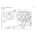
2.1.1 Block Diagram
2.1.2 Pin Connections and short description
Pin No.
Pin Name
I/O
Pin Function
sheet name
B16
GPIO07
O
General purpose I/O port GPIO07
U_D_OUT
A16
GPIO06
O
General purpose I/O port GPIO06
L_R_OUT
D15
GPIO05
O
General purpose I/O port GPIO05
open
C15
GPIO04
O
General purpose I/O port GPIO04
PDN
B15
GPIO03
O
General purpose I/O port GPIO03
INV-POWER
A15
GPIO02
O
General purpose I/O port GPIO02
A-SW1
D14
GPIO01
O
General purpose I/O port GPIO01
A-SW2
C14
GPIO00
O
General purpose I/O port GPIO00
AD-RESET
B14
GPIO17
O
General purpose I/O port GPIO17
F-RESET
A14
GPIO16
O
General purpose I/O port GPIO16
WP-CONT
C13
GPIO15
I
General purpose I/O port GPIO15
HPD
B13
GPIO14
O
General purpose I/O port GPIO14
HPD-CTRL
A13
GPIO13
I
General purpose I/O port GPIO13
D-CONNECT
C12
GPIO12
I
General purpose I/O port GPIO12
SSW
B12
GPIO11
I
General purpose I/O port GPIO11
HP-DET
A12
GPIO10
O
General purpose I/O port GPIO10
open
D11
GPIO27
O
General purpose I/O port GPIO27
HP-MUTE
C11
GPIO26
O
General purpose I/O port GPIO26
SPDIF-MUTE
B11
GPIO25
O
General purpose I/O port GPIO25
DTV-SEL
A11
GPIO24
O
General purpose I/O port GPIO24
MPSEL-OUT
D10
GPIO23
O
General purpose I/O port GPIO23
AMP-HOGO
C10
GPIO22
O
General purpose I/O port GPIO22
open
B10
GPIO21
O
General purpose I/O port GPIO21
SCART-MUTE
A10
GPIO20
I
General purpose I/O port GPIO20
I2C-GATE
L22
GPIO37
O
General purpose I/O port GPIO37
DTV_D_A_SEL
L23
GPIO36
O
General purpose I/O port GPIO36
DTV_INT
K20
GPIO35
O
General purpose I/O port GPIO35
A-MUTE-ENABLE
K21
GPIO34
I
General purpose I/O port GPIO34
B5V
K22
GPIO33
O
General purpose I/O port GPIO33
ANT-POWER
LC-19A1E-BK/WH
5 – 4
K23
GPIO32
O
General purpose I/O port GPIO32
SMT-CMD
J20
GPIO31
O
General purpose I/O port GPIO31
SMT-RST
J21
GPIO30
O
General purpose I/O port GPIO30
CLK-SEL
J22
GPIO47
O
General purpose I/O port GPIO47
DTV_CS
J23
GPIO46
O
General purpose I/O port GPIO46
DTV_CLOCK
H20
GPIO45
O
General purpose I/O port GPIO45
DTV_DO
H21
GPIO44
O
General purpose I/O port GPIO44
DTV_DI
H22
GPIO43
O
General purpose I/O port GPIO43
SP-MUTE
H23
GPIO42
O
General purpose I/O port GPIO42
L-MUTE
G20
GPIO41
O
General purpose I/O port GPIO41
DTV_RESET
G21
GPIO40
O
General purpose I/O port GPIO40
DTV_POWER
G22
GPIO57
I
General purpose input and output portGPIO57 at BUSOPEN= “L”, MPSEL0=
“L”, MPSEL1= “L”
“L”, MPSEL1= “L”
DVP-REQ (IN)
G23
GPIO56/SCLK2
I
General purpose input and output portGPIO56 at BUSOPEN= “L”, MPSEL0=
“L”, MPSEL1= “L” or BUSOPEN= “H”, MPSEL0= “L”, MPSEL1= “H”
“L”, MPSEL1= “L” or BUSOPEN= “H”, MPSEL0= “L”, MPSEL1= “H”
DVP_CLK
F20
GPIO55/TXD2
O
General purpose input and output portGPIO55/UART2 transmit data at BUSO-
PEN= “L”, MPSEL0= “L”, MPSEL1= “L” or BUSOPEN= “H”, MPSEL0= “L”,
MPSEL1= “H”
PEN= “L”, MPSEL0= “L”, MPSEL1= “L” or BUSOPEN= “H”, MPSEL0= “L”,
MPSEL1= “H”
DVP_TXD
F21
GPIO54/RXD2
I
General purpose input and output portGPIO53/UART2 receive data at BUSO-
PEN= “L”, MPSEL0= “L”, MPSEL1= “L” or BUSOPEN= “H”, MPSEL0= “L”,
MPSEL1= “H”
PEN= “L”, MPSEL0= “L”, MPSEL1= “L” or BUSOPEN= “H”, MPSEL0= “L”,
MPSEL1= “H”
DVP_RXD
C17
GPIO53
I
General purpose input and output port GPIO53/
E2P-STOP
B17
GPIO52
I/O
General purpose input and output port GPIO52
SMT_SEL
A17
GPIO51
I/O
General purpose input and output port GPIO51
SMTD_0
C16
GPIO50
I/O
General purpose input and output port GPIO50
SMTD_1
A6
GPIO67/SCL0
I
General purpose input and output port GP GPIO67/I2C-bus 0 interface transfer
clock.
clock.
SCL1
B6
GPIO66/SDA0
I/O
General purpose input and output port GPIO66/
I2C-bus 0 interface transmit/ receive data
I2C-bus 0 interface transmit/ receive data
SDA1
B5
GPIO65/SCL1
I
General purpose input and output port GPIO65/
I2C-bus 1 interface transfer clock.
I2C-bus 1 interface transfer clock.
SCL2
C5
GPIO64/SDA1
I/O
General purpose input and output port GPIO64/
I2C-bus 1 interface transmit/receive data.
I2C-bus 1 interface transmit/receive data.
SDA2
C4
GPIO63/SCL2
I
General purpose input and output port GPIO63/
I2C-bus 2 interface transfer clock.
I2C-bus 2 interface transfer clock.
SCL3
A5
GPIO62/SDA2
I/O
General purpose input and output port GPIO62/
I2C-bus 2 interface transmit/receive data.
I2C-bus 2 interface transmit/receive data.
SDA3
B7
GPIO61/INT0
I
General purpose input and output port GPIO61/External interruption terminal 0
DVP-INT (IN)
A7
GPIO60/INT1
I
General purpose input and output port GPIO60/External interruption terminal 1
ICC-INT
C6
INT2
I
External interruption terminal 2
DTV_REQ/ERR
C9
TCK
I
Clock for SDI
JTAG-TCK
B9
TDI
I
Data input for SDI
JTAG-TDI
A9
TDO
O
Data output for SDI
JTAG-TDO
C7
TMS
I
Mode select for SDI
JTAG-TMS
C8
TRS
I
Reset for SDI
JTAG-TRS
B4
TRDATA0
I
Trace data 0 for SDI
TRDATA0
A4
TRDATA1
I
Trace data 1 for SDI
TRDATA1
C3
TRDATA2
I
Trace data 2 for SDI
TRDATA2
B3
TRDATA3
I
Trace data 3 for SDI
TRDATA3
A3
TRDATA4
I
Trace data 4 for SDI
TRDATA4
C2
TRDATA5
I
Trace data 5 for SDI
TRDATA5
B2
TRDATA6
I
Trace data 6 for SDI
TRDATA6
A2
TRDATA7
I
Trace data 7 for SDI
TRDATA7
C1
TRSYNC
I
Trace synchronizing signal for SDI
TRSYNC
B1
TRCLK
I
Trace clock signal for SDI
TRCLK
AB1
PXD00
I
Digital video signal input 00 (A)
open
Y2
PXD01
I
Digital video signal input 01 (A)
open
AA2
PXD02
I
Digital video signal input 02 (A)
HDMI_B
AB2
PXD03
I
Digital video signal input 03 (A)
HDMI_B
AC2
PXD04
I
Digital video signal input 04 (A)
HDMI_B
AA3
PXD05
I
Digital video signal input 05 (A)
HDMI_B
AB3
PXD06
I
Digital video signal input 06 (A)
HDMI_B
AC3
PXD07
I
Digital video signal input 07 (A)
HDMI_B
AA4
PXD08
I
Digital video signal input 08 (A)
HDMI_B
AB4
PXD09
I
Digital video signal input 09 (A)
HDMI_B
AC4
PXD10
I
Digital video signal input 10 (B)
NC
Pin No.
Pin Name
I/O
Pin Function
sheet name

