Sharp LC-19A1E (serv.man5) Service Manual ▷ View online
LC-19A1E-BK/WH
5 – 29
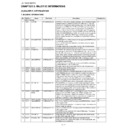
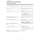
2.17.2 Pin Connections and short description
Pin No.
Pin Name
I/O
Pin Function
1
V1-V
I
Video input terminal
(Composite or Y)
*Sync chip clamp
(Composite or Y)
*Sync chip clamp
3
V1-Y
7
V2-V
9
V2-Y
13
V3-V
16
STV-V
19
YIN2
32
YIN1
41
MTV-V
2
V1-L
I
Audio input terminal
4
V1-R
8
V2-L
10
V2-R
14
V3-L
15
V3-R
17
STV-L
18
STV-R
40
MTV-R
42
MTV-L
5
V1-C
I
Video input terminal
(Croma)
(Croma)
11
V2-C
21
CIN2
31
CIN1
6
S1
I
Distinction 3-effects input terminal
12
S2
DC Detect
20
ADR
I
Sleve address select
30
MUTE
Audio Mute terminal
27
GND
-
Ground.
22
VOUT2
O
Composite video out
35
VOUT1
23
ROUT2
O
Audio out terminal
25
LOUT2
33
ROUT1
34
LOUT1
24
COUT2
O
S-Video out terminal
26
YOUT2
37
YOUT1
39
COUT1
28
SDA
I/O
Data input from I2C
29
SCL
I
CLK input from I2C
36
BIAS
I
Internal bias terminal
38
VCC
-
Power Supply.
LC-19A1E-BK/WH
5 – 30
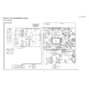
2.18. IC502 (VHiiSL83220-1Y)
2.18.1 Block Diagram
2.18.2 Pin Connections and short description
Pin No.
Pin Name
I/O
Pin Function
15
VCC
-
System power supply input (3.0V to 5.5V)
3
V+
-
Intemally generated positive transmitter supply (+5.5V).
7
V-
-
Internally generated negative transmitter supply (-5.5V).
14
GND
-
Ground connection.
2
C1+
-
External capacitor (voltage doubler) is connected to this lead.
4
C1-
-
External capacitor (voltage doubler) is connected to this lead.
5
C2+
-
External capacitor (voltage doubler) is connected to this lead.
6
C2-
-
External capacitor (voltage doubler) is connected to this lead.
11
TIN
I
TTL/CMOS compatible transmitter inputs.
13
TOUT
O
±15KV ESD Protected, RS-232 level (nominally ±5.5V) transmitter output.
8
RIN
I
±15KV ESD Protected, RS-232 compatible receiver inputs.
9
ROUT
O
TTL/CMOS level receiver output.
1
EN
O
Active low receiver enable control; doesn't disable ROUTB output.
16
SHDN
-
Active low input shuts down transmitters and on-board power supply, to place device in low power mode.
10
N.C.
-
No internal connection.
LC-19A1E-BK/WH
5 – 31
2.19. IC7501 (VHiBD9883FV)
2.19.1 Block Diagram
2.19.2 Pin Connections and short description
Pin No.
Pin Name
I/O
Pin Function
1
DUTY
I
Switch terminal of PWM mode and BURST mode.
2
BCT
-
Capacity connecting terminal for setting BURST oscillator frequency.
3
BRT
-
Resistance connecting terminal for setting the charge and discharge current of BCT terminal
4
CT
-
Capacity connecting terminal for setting Oscillator Frequency.
5
RT
-
Resistance connecting terminal for setting the charge and discharge current of CT terminal.
6
SRT
-
Resistance connecting terminal for setting the charge and discharge current of CT terminal.
7
GND
-
Ground.
8
FB
O
Error amplifier output. (FB)
9
IS
I
Error amplifier input 1. (IS)
10
VS
I
Error amplifier input 2. (VS)
11
STB
I
stand-by switch terminal.
12
SCP
-
Capacity connecting terminal for setting SCP timer.
13
SS
O
Capacity connecting terminal for setting soft start.
14
PGND
-
GND terminal of a built-out FET drive circuit.
15
LN
O
The output terminal of a bult-out FET drive circuit. (LN)
16
HN
O
The output terminal of a bult-out FET drive circuit. (HN)
17
SW
O
Low voltage rail terminal for HN output. (Earth)
18
BST
I
Boot-Strap input terminal for HN output.
19
REG
O
The output voltage terminal of an internal regulator circuit.
20
VCC
-
Supply voltage input.

