Sharp XL-60 (serv.man20) Service Manual ▷ View online
– 51 –
XL-60H/70H
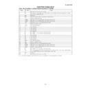
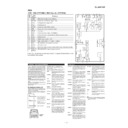
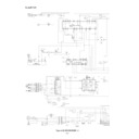
IC804 VHiLA6541D/-1: Focus/Tracking/Spin/Sled Driver (LA6541D)
In this unit, the terminal with asterisk mark (*) is (open) terminal which is not connected to the outside.
IC804 VHiLA6541D/-1: Focus/Tracking/Spin/Sled Driver (LA6541D)
Figure 51 BLOCK DIAGRAM OF IC
1
VCC
Power (short-circuited to pin 30)
2
MUTE
All BTL AMP output ON/OFF
3
VIN1
BTL AMP1 input terminal
4
VG1
BTL AMP1 input terminal (for gain adjustment)
5
VO1
BTL AMP1 output terminal (noninversion side)
6
VO2
BTL AMP1 output terminal (inversion side)
7
GND
GND terminal (lowest potential)
8
GND
GND terminal (lowest potential)
9
GND
GND terminal (lowest potential)
10
VO3
Output terminal of BTL AMP2 (inversion side)
11
VO4
Output terminal of BTL AMP2 (noninversion side)
12
VG2
Input terminal of BTL AMP2 (for gain adjustment)
13
VIN2
Input terminal of BTL AMP2
14
REG OUT
Connect the collector of externally provided transistor (PNP). 5V power output
15
REG IN
Connect the base of externally provided transistor (PNP).
16*
RES
Reset output
17*
CD
Reset output delay time setting (capacitor provided externally)
18
VIN3
Input terminal of BTL AMP3
19*
VG3
Input terminal of BTL AMP3 (for gain adjustment)
20
VO5
Output terminal of BTL AMP3 (noninversion side)
21
VO6
Output terminal of BTL AMP3 (inversion side)
22
GND
GND terminal (lowest potential)
23
GND
GND terminal (lowest potential)
24
GND
GND terminal (lowest potential)
25
VO7
Output terminal of BTL AMP4 (inversion side)
26
VO8
Output terminal of BTL AMP4 (noninversion side)
27
VG4
Input terminal of BTL AMP4 (for gain adjustment)
28
VIN4
Input terminal of BTL AMP4
29
VREF
Application of standard voltage of level shift circuit
30
VCC
Power (short-circuited to pin 1)
Pin No.
Port Name
Function
*GND (lowest potential) is connected to the frame of pin center.
1
2
3
4
5
6
7
8
9
10
11
12
13
14
15
30
29
28
27
26
25
24
23
22
21
20
19
18
17
16
11k
Ω
11k
Ω
11k
Ω
11k
Ω
VCC
Mute
VIN1
VG1
Vo1
Vo2
GND
GND
GND
Vo3
Vo4
VG2
VIN2
Reg OUT
Reg IN
VCC
Vref
VIN4
VG4
Vo8
Vo7
GND
GND
GND
Vo6
Vo5
VG3
VIN3
CD
RES
Level shift
1
Level shift
4
Level shift
2
Level shift
3
1
4
BTL AMP
BTL AMP
2
3
BTL AMP
BTL AMP
Regulator
RESET
Vcc

