Sharp XL-1100 (serv.man10) Service Manual ▷ View online
– 57 –
XL-1000H/1100H
39
AVDD
Input
Analog system power terminal.
40
RFCT
Input
RFRP signal center level input terminal.
41
RFZI
Input
RFRP zero cross input terminal.
42
RFRP
Input
RF ripple signal input terminal.
43
FEI
Input
Focus error signal input terminal.
44
SBAD
Input
Sub-beam addition signal input terminal.
45
TSIN
Input
Test input terminal. To be fixed to Vref usually.
46
TEI
Input
Tacking error input terminal. (Tracking servo ON: Taking-in).
47
TEZI
Input
Tracking error, zero cross input termina.l
48
FOO
Output
Focus equalizer output terminal.
49
TRO
Output
Tracking equalizer output terminal.
50
VREF
Input
Analog standard power terminal.
51
RFGC
Output
RF amplitude adjustment control signal output terminal.
3-value PWM signal is output. (PWM carrier = 88.2 kHz)
3-value PWM signal is output. (PWM carrier = 88.2 kHz)
52
TEBC
Output
Tracking balance control signal output terminal.
3-value PWM signal is output. (PWM carrier = 88.2 kHz)
3-value PWM signal is output. (PWM carrier = 88.2 kHz)
53
FMO
Output
Feed equalizer output terminal. 3-value PWM signal is output. (PWM carrier = 88.2 kHz)
54*
FVO
Output
Speed error signal or feed search EQ output terminal.
3-value PWM signal is output. (PWM carrier = 88.2 kHz)
3-value PWM signal is output. (PWM carrier = 88.2 kHz)
55
DMO
Output
Disc equalizer output terminal.
3-value PWM signal is output. (PWM carrier = DSP system 88.2 kHz, sync with PXO)
3-value PWM signal is output. (PWM carrier = DSP system 88.2 kHz, sync with PXO)
56
2VREF
Input
Analog standard power terminal (2xVREF)
57
SEL
Output
APC circuit ON/OFF signal output terminal.
When laser is ON and UHS = L, "Hi-Z". When UHS = H, "H" output is obtained.
When laser is ON and UHS = L, "Hi-Z". When UHS = H, "H" output is obtained.
58*
FLGA
Output
Internal signal monitor external flag output terminal.
TEZC, FOON, FOK and RFZC signals can be selected with command.
TEZC, FOON, FOK and RFZC signals can be selected with command.
59*
FLGB
Output
Internal signal monitor external flag output terminal.
DFCT, FOON, FMON and RFZC signals can be selected with command.
DFCT, FOON, FMON and RFZC signals can be selected with command.
60*
FLGC
Output
Internal signal monitor external flag output terminal.
TRON, TRSR, FOK, and SRCH signals can be selected with command.
TRON, TRSR, FOK, and SRCH signals can be selected with command.
61*
FLGD
Output
Internal signal monitor external flag output terminal.
TRON, DMON, HYS and SHC signals can be selected with command.
TRON, DMON, HYS and SHC signals can be selected with command.
62
VDD
Input
Digital + power terminal.
63
VSS
—
Digital ground terminal.
64*
IO0
Input/Output
General-use I/O port.
65*
IO1
The input port and output port can be selected with command. In case of input port the terminal
66*
IO2
state (H/L) can be read with the read command.
67*
IO3
In case of output port the terminal state (H/L/HiZ) can be controlled with command.
68*
/DMOUT
Input
Terminal to set the mode to output 2-value PWM of feed equalizer from IO0,1 terminal and 2-
value PWM of disc equalizer from IO2,3 terminal. "L" active
value PWM of disc equalizer from IO2,3 terminal. "L" active
69*
/CKSE
Input
To be opened usually.
70*
/DACT
Input
DAC test mode terminal. To be opened usually.
71
TESIN
Input
Test input terminal (externally provided VCO clock input terminal). To be fixed to "L" usually.
72
TESIO1
Input
Test input/output terminal. To be fixed to "L" usually.
73
VSS
—
Digital ground terminal.
74
PXI
Input
DSP system clock oscillation circuit input terminal. To be fixed to "L" usually.
75*
PXO
Output
DSP system clock oscillation circuit output terminal.
76
VDD
Input
Digital + power terminal.
77
XVSS
—
System clock oscillation circuit ground terminal.
78
XI
Input
System clock oscillation input terminal.
79
XO
Output
System clock oscillation circuit output terminal.
80
XVDD
Input
System clock oscillation circuit + power terminal.
81
DVSR
Input
R channel D/A converting section power terminal.
82
RO
Output
R channel data forward rotation output terminal.
IC802 VHiTC9462F/-1: Servo/Signal Control (TC9462F) (2/3)
Pin No.
Port Name
Function
Input/Output
In this unit, the terminal with asterisk mark (*) is (open) terminal which is not connected to the outside.
XL-1000H/1100H
– 58 –
83
DVDD
Input
D/A converting section power terminal.
84
DVR
Input
Reference voltage terminal.
85
LO
Output
L channel data forward rotation output terminal.
86
DVSL
Input
L channel D/A converting section power terminal.
87*
TEST1
Input
Test mode terminal. To be opened usually.
88*
TEST2
Input
Test mode terminal. To be opened usually.
89*
TEST3
Input
Test mode terminal. To be opened usually.
90-93
BUS0-BUS3
Input/Output
Microcomputer interface data input/output terminal.
94
VDD
Input
Digital + power terminal.
95
VSS
—
Digital ground terminal.
96
BUCK
Input
Microcomputer interface clock input terminal.
97
/CCE
Input
Microcomputer interface chip enable signal input terminal. "L": BUS0 to 3 is active.
98*
TEST4
Input
Test mode termina. To be opened usually.
99*
/TSMOD
Input
Local test mode selection terminal.
100
/RST
Input
Reset signal input terminal. "L": Reset.
IC802 VHiTC9462F/-1: Servo/Signal Control (TC9462F) (3/3)
Pin No.
Port Name
Function
Input/Output
In this unit, the terminal with asterisk mark (*) is (open) terminal which is not connected to the outside.
IC802 VHiTC9462F/-1: Servo/Signal Control (TC9462F)
2
3
4
5
1
7
8
9
6
12
13
14
15
11
17
18
19
10
16
22
23
24
25
21
27
28
29
20
30
26
42
43
44
45
41
47
48
49
50
46
32
33
34
35
31
37
38
39
40
36
89
88
87
86
90
84
83
82
81
85
99
98
97
96
100
94
93
92
91
95
72
73
74
75
71
77
78
79
70
80
76
62
63
64
65
61
67
68
69
60
66
52
53
54
55
51
57
58
59
56
LPF
1Bit
DAC
Microcomputer
interface
Correction
circuit
Audio output
circuit
Digital
out
16KRAM
Sub-code
demodulation
circuit
Status
PLL
TMAX
VCO
Data
slicer
CLV
servo
D/A
PWM
Servo control
ROM
RAM
Digital equalizer
adjustment circuit
Address
circuit
Clock
generator
/RST
/TSMOD
TEST4
/CCE
BUCK
VSS
VDD
BUS3
BUS2
BUS1
BUS0
TEST3
TEST2
TEST1
DVSL
LO
DVR
DVDD
RO
DVSR
LPFN
LPFO
PVREF
VCOREF
VCOF
AVSS
SLCO
RFI
AVDD
RFCT
RFZI
RFRP
FEI
SBAD
TSIN
TEI
TEZI
FOO
TRO
VREF
TMAX
TMAXS
PDO
ZDET
HSSW
P2VREF
TESIO0
VDD
MONIT
COFS
SPDA
SPCK
SBSY
SFSY
DATA
VSS
VDD
CLCK
SBOK
IPF
MBOV
DOUT
AOUT
BCK
VSS
LRCK
EMPH
/UHSO
/HSO
TEST0
RFGC
TEBC
FMO
FVO
DMO
2VREF
SEL
FLGA
FLGB
FLGC
FLGD
VDD
VSS
IO0
IO1
IO2
IO3
/DMOUT
/CKSE
/DACT
TESIN
TESIO1
VSS
PXI
PXO
VDD
XVSS
XI
XO
XVDD
Synchronizing
signal guarantee
EFM demodulation
A/D
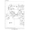
Figure 58 BLOCK DIAGRAM OF IC
– 59 –
XL-1000H/1100H
IC804 VHiMM1469XH-1: Focus/Tracking/Spin/Sled Driver (MM1469XH)
In this unit, the terminal with asterisk mark (*) is (open) terminal which is not connected to the outside.
1
CH1-OUT-A
Driver CH1 negative output
2
CH1-OUT-B
Driver CH1 positive output
3
CH1-IN-A
Driver CH1 input
4
CH1-IN-B
Driver CH1 input, gain adjustment pin
5
Tr-B
Connect to external transistor base
6
VREG-OUT
Constant voltage output, connects to external transistor collector
7
MUTE
Driver mute control input
8
GND
GND
9
CH2-IN-B
Driver CH2 input, gain adjustment pin
10
CH2-IN-A
Driver CH2 input
11
CH2-OUT-B
Driver CH2 positive output
12
CH2-OUT-A
Driver CH2 negative output
13
Substrate GND
Substrate GND
14*
OP-OUT
Operational amplifier output
15*
OP-IN(–)
Operational amplifier input, negative
16*
OP-IN(+)
Operational amplifier input, positive
17
CH3-OUT-A
Driver CH3 negative output
18
CH3-OUT-B
Driver CH3 positive output
19
CH3-IN-A
Driver CH3 input
20*
CH3-IN-B
Driver CH3 input, gain adjustment pin
21
Vcc
Vcc
22
Vcc
Vcc
23
BIAS-IN
Bias amplifier input
24
CH4-IN-B
Driver CH4 input, gain adjustment pin
25
CH4-IN-A
Driver CH4 input
26
CH4-OUT-B
Driver CH4 positive output
27
CH4-OUT-A
Driver CH4 negative output
28
Substrate GND
Substrate GND
Pin No.
Port Name
Function
GND (lowest potential) is connected to the frame of pin center.
1
2
3
4
5
6
7
8
9
10
11
12
13
14
15
28
27
26
D.BUF
OP-IN(–)
OP-IN(+)
CH3-OUT-A
CH3-OUT-B
CH3-IN-A
CH3-IN-B
Vcc
Vcc
BIAS-IN
CH4-IN-B
CH4-IN-A
CH4-OUT-B
CH4-OUT-A
SUBGND
OP-OUT
SUBGND
CH2-OUT-A
CH2-OUT-B
CH2-IN-A
CH2-IN-B
GND
MUTE
VREG-OUT
Tr-B
CH1-IN-B
CH1-IN-A
CH1-OUT-B
CH1-OUT-A
D.BUF D.BUF
D.BUF D.BUF
D.BUF
VCC
VCC
D.BUF
D.BUF : Driver Buffer
T.S.D : Thermal Shut Down
D.BUF
DRIVER MUTE
Level shift
25
24
23
22
21
20
19
18
17
16
10k
Ω
50k
Ω
50k
Ω
10k
Ω
10k
Ω
10k
Ω
T.S.D
Level shift
10k
Ω
Level shift
10k
Ω
Level shift
Figure 59 BLOCK DIAGRAM OF IC
XL-1000H/1100H
– 60 –
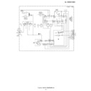
LCD701: RV-LX0014SJZZ LCD Display (XL-1000H)
LCD701: RV-LX0012SJZZ LCD Display (XL-1100H)
LCD701: RV-LX0012SJZZ LCD Display (XL-1100H)
Figure 60 LCD SEGMENT
PinNo
1
2
3
4
5
6
7
8
9
10
11
12
13
14
15
16
17
18
19
20
21
com1
com1
z1
h1
g1
a1
REC
h2
g2
a2
SLEEP
h3
g3
a3
RANDOM
h4
g4
a4
MEMORY
com2
com2
b1
j1
n1
p1
b2
j2
n2
p2
b3
j3
n3
p3
b4
j4
n4
p4
b5
com3
com3
c1
l1
m1
f1
c2
l2
m2
f2
c3
l3
m3
f3
c4
l4
m4
f4
c5
com4
com4
z2
k1
d1
e1
z3
k2
d2
e2
MHz
k3
d3
e3
kHz
k4
d4
e4
z4
PinNo
22
23
24
25
26
27
28
29
30
31
32
33
34
35
36
37
38
39
40
41
42
com1
h5
g5
a5
RDS
h6
g6
a6
r
h7
g7
a7
TP
h8
g8
a8
EON
com1
com2
j5
n5
p5
b6
j6
n6
p6
b7
j7
n7
p7
b8
j8
n8
p8
PTY
com2
com3
l5
m5
f5
c6
l6
m6
f6
c7
l7
m7
f7
c8
l8
m8
f8
TI
com3
com4
k5
d5
e5
ST
k6
d6
e6
q
k7
d7
e7
k8
d8
e8
TA
SRS(0)
com4
z1
z2
z3
r
q
z4
1 2 3 4 5 6 7 8 9 10 11 12 13 14 15 16 17 18 19 20 21 22 23 24 25 26 27 28 29 30 31 32 33 34 35 36 37 38 39 40 41 42

