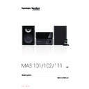
Harman Kardon MAS 101-102-111 (serv.man3) Service Manual ▷ View online
Pin Assignments
*With package soldered to 0.5 square inch copper area over backside ground plane or internal power plane.,
Θ
JA
can vary from
30°C/W to more than 50°C/W. Other mounting techniques may provide better thermal resistance than 30°C/W.
Absolute Maximum Ratings
Figure 1. Absolute Maximum Safe Operating Area
Parameter
Min.
Max.
Unit
V
IN
18
V
(V
IN
– V
OUT
) * I
OUT
See Figure 1
Operating Junction Temperature Range
0
125
°
C
Storage Temperature Range
-65
150
°
C
Lead Temperature (Soldering, 10 sec.)
300
°
C
Front View
Front View
4-Lead Plastic SOT-223
Θ
JC
= 15
°
C/W*
3-Lead Plastic TO-252
Θ
JC
= 3
°
C/W*
Tab is
V
OUT
Tab is V
OUT
1
GND
OUT
IN
2
3
3
2
1
IN
OUT
GND
1.2
1.0
0.8
0.6
0.4
0.2
0
0
6
8
10
12
14
16
18
20
4
2
V
IN
– V
OUT
(V)
I
OUT
(A)
27
1. General
description
The HEF4094B is an 8-stage serial shift register. It has a storage latch associated with
each stage for strobing data from the serial input to parallel buffered 3-state outputs
QP0 to QP7. The parallel outputs may be connected directly to common bus lines. Data is
shifted on positive-going clock transitions. The data in each shift register stage is
transferred to the storage register when the strobe (STR) input is HIGH. Data in the
storage register appears at the outputs whenever the output enable (OE) signal is HIGH.
Two serial outputs (QS1 and QS2) are available for cascading a number of HEF4094B
devices. Serial data is available at QS1 on positive-going clock edges to allow high-speed
operation in cascaded systems with a fast clock rise time. The same serial data is
available at QS2 on the next negative going clock edge. This is used for cascading
HEF4094B devices when the clock has a slow rise time.
It operates over a recommended V
DD
power supply range of 3 V to 15 V referenced to V
SS
(usually ground). Unused inputs must be connected to V
DD
, V
SS
, or another input. It is
also suitable for use over the industrial (
−40 °C to +85 °C) and automotive (−40 °C to
+125
°C) temperature ranges.
2. Features and benefits
Fully static operation
5 V, 10 V, and 15 V parametric ratings
Standardized symmetrical output characteristics
Operates across the automotive temperature range
−40 °C to +125 °C
Complies with JEDEC standard JESD 13-B
3. Ordering
information
HEF4094B
8-stage shift-and-store register
Rev. 08 — 2 April 2010
Product data sheet
Table 1.
Ordering information
All types operate from
−
40
°
C to +125
°
C.
Type number
Package
Name
Description
Version
HEF4094BP
DIP16
plastic dual in-line package; 16 leads (300 mil)
SOT38-4
HEF4094BT
SO16
plastic small outline package; 16 leads; body width 3.9 mm
SOT109-1
HEF4094BTS
SSOP16
plastic shrink small outline package; 16 leads; body width 5.3 mm
SOT338-1
28
NXP Semiconductors
HEF4094B
8-stage shift-and-store register
4. Functional
diagram
Fig 1.
Functional diagram
Fig 2.
Logic symbol
001aaf119
8-STAGE SHIFT
REGISTER
8-BIT STORAGE
REGISTER
3-STATE OUTPUTS
D
2
QS2
10
QS1
QP0
4
5
6
7
14
13
12
11
QP1 QP2 QP3 QP4 QP5 QP6
QP7
9
CP
3
STR
1
OE
15
15
2
OE
D
CP
STR
3
1
QP0
QP1
QP2
QP3
QP4
QP5
QP6
QP7
QS1
QS2
9
10
4
5
6
7
14
13
12
11
001aaf111
Fig 3.
Logic diagram
001aag799
D
D
CP
CP
Q
FF 0
D
LE
Q
LATCH 0
D
CP
Q
FF 7
D
LE
Q
LATCH 7
D
CP
Q
STAGES 1 TO 6
STAGE 0
STAGE 7
QP2
QP0
D
QS2
QS1
LE
Q
LATCH
QP1
QP4
QP3
QP6
QP5
QP7
STR
OE
29
NXP Semiconductors
HEF4094B
8-stage shift-and-store register
5. Pinning
information
5.1 Pinning
5.2 Pin description
Fig 4.
Pin configuration
HEF4094B
STR
V
DD
D
OE
CP
QP4
QP0
QP5
QP1
QP6
QP2
QP7
QP3
QS2
V
SS
QS1
001aae662
1
2
3
4
5
6
7
8
10
9
12
11
14
13
16
15
Table 2.
Pin description
Symbol
Pin
Description
STR
1
strobe input
D
2
data input
CP
3
clock input
QP0 to QP7
4, 5, 6, 7, 14, 13, 12, 11
parallel output
V
SS
8
ground supply voltage
QS1
9
serial output
QS2
10
serial output
OE
15
output enable input
V
DD
16
supply voltage
30
Click on the first or last page to see other MAS 101-102-111 (serv.man3) service manuals if exist.

