Sony DCR-IP5 / DCR-IP5E / DCR-IP7BT / DCR-IP7E Service Manual ▷ View online
DIGITAL VIDEO CAMERA RECORDER
The information that is not described in this
Service Manual is described in the LEVEL 2
Service Manual.
When repairing, use this manual together with
LEVEL 2 Service Manual.
Service Manual is described in the LEVEL 2
Service Manual.
When repairing, use this manual together with
LEVEL 2 Service Manual.
Contents of LEVEL 2 Service Manual
SERVICE NOTE
1. GENERAL
2. DISASSEMBLY
3. BLOCK DIAGRAMS
4. PRINTED WIRING BOARDS AND
SCHEMATIC DIAGRAMS
5. ADJUSTMENTS
6. REPAIR PARTS LIST
OVERALL
POWER
LD-105 BOARD
CONTROL SWITCH BLOCK (CF-1900),(FK-1900)
FP-140, FP-141, FP-228 FLEXIBLE BOARD
VF-149 BOARD
JK-209 BOARD
FP-366 FLEXIBLE BOARD
PD-142 BOARD
EXPLODED VIEWS
ELECTRICAL PARTS LIST
SERVICE MANUAL
SERVICE MANUAL
Level 3
DCR-IP5/IP5E/IP7BT/IP7E
RMT-817/818
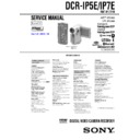
Photo : DCR-IP7E
RMT-817
US Model
Canadian Model
DCR-IP5/IP7BT
AEP Model
UK Model
DCR-IP5E/IP7E
E Model
Hong Kong Model
DCR-IP5/IP5E/IP7E
Tourist Model
DCR-IP5/IP5E
Australian Model
DCR-IP7E
Korea Model
DCR-IP5
V MECHANISM
Ver 1.2 2005. 06
— 2 —
SAFETY-RELATED COMPONENT WARNING!!
COMPONENTS IDENTIFIED BY MARK
0
OR DOTTED LINE WITH
MARK
0
ON THE SCHEMATIC DIAGRAMS AND IN THE PARTS
LIST ARE CRITICAL TO SAFE OPERATION. REPLACE THESE
COMPONENTS WITH SONY PARTS WHOSE PART NUMBERS
APPEAR AS SHOWN IN THIS MANUAL OR IN SUPPLEMENTS
PUBLISHED BY SONY.
COMPONENTS WITH SONY PARTS WHOSE PART NUMBERS
APPEAR AS SHOWN IN THIS MANUAL OR IN SUPPLEMENTS
PUBLISHED BY SONY.
ATTENTION AU COMPOSANT AYANT RAPPORT
À LA SÉCURITÉ!
LES COMPOSANTS IDENTIFÉS PAR UNE MARQUE
0
SUR LES
DIAGRAMMES SCHÉMATIQUES ET LA LISTE DES PIÈCES SONT
CRITIQUES POUR LA SÉCURITÉ DE FONCTIONNEMENT. NE
REMPLACER CES COMPOSANTS QUE PAR DES PIÈSES SONY
DONT LES NUMÉROS SONT DONNÉS DANS CE MANUEL OU
DANS LES SUPPÉMENTS PUBLIÉS PAR SONY.
CRITIQUES POUR LA SÉCURITÉ DE FONCTIONNEMENT. NE
REMPLACER CES COMPOSANTS QUE PAR DES PIÈSES SONY
DONT LES NUMÉROS SONT DONNÉS DANS CE MANUEL OU
DANS LES SUPPÉMENTS PUBLIÉS PAR SONY.
1.
Check the area of your repair for unsoldered or poorly-soldered
connections. Check the entire board surface for solder splashes
and bridges.
connections. Check the entire board surface for solder splashes
and bridges.
2.
Check the interboard wiring to ensure that no wires are
"pinched" or contact high-wattage resistors.
"pinched" or contact high-wattage resistors.
3.
Look for unauthorized replacement parts, particularly
transistors, that were installed during a previous repair. Point
them out to the customer and recommend their replacement.
transistors, that were installed during a previous repair. Point
them out to the customer and recommend their replacement.
4.
Look for parts which, through functioning, show obvious signs
of deterioration. Point them out to the customer and
recommend their replacement.
of deterioration. Point them out to the customer and
recommend their replacement.
5.
Check the B+ voltage to see it is at the values specified.
6.
Flexible Circuit Board Repairing
• Keep the temperature of the soldering iron around 270˚C
during repairing.
• Do not touch the soldering iron on the same conductor of the
circuit board (within 3 times).
• Be careful not to apply force on the conductor when soldering
or unsoldering.
SAFETY CHECK-OUT
After correcting the original service problem, perform the following
safety checks before releasing the set to the customer.
DCR-IP5/IP5E/IP7BT/IP7E
TABLE OF CONTENTS
4.
PRINTED WIRING BOARDS AND
SCHEMATIC DIAGRAMS
SCHEMATIC DIAGRAMS
4-2.
PRINTED WIRING BOARDS AND
SCHEMATIC DIAGRAMS ·········································· 4-11
SCHEMATIC DIAGRAMS ·········································· 4-11
• VC-263 (A/D CONVERTER, TIMING GENERATOR,
CAMERA/DV SIGNAL PROCESS, LENS CONTROL,
CHARACTER GENERATOR, VIDEO BUFFER,
DIGITAL STILL CONTROL, MPEG VIDEO
PROCESS, i LINK I/F, MPEG AUDIO, Q PROCESS,
HEAD AMP, PLL, VIDEO I/O, MIC DRIVE,
HI/MECHANISM CONTROL, DRAM/CAPSTAN
MOTOR DRIVE, AUDIO PROCESS, CONNECTOR,
DC/DC CONVERTER)
CHARACTER GENERATOR, VIDEO BUFFER,
DIGITAL STILL CONTROL, MPEG VIDEO
PROCESS, i LINK I/F, MPEG AUDIO, Q PROCESS,
HEAD AMP, PLL, VIDEO I/O, MIC DRIVE,
HI/MECHANISM CONTROL, DRAM/CAPSTAN
MOTOR DRIVE, AUDIO PROCESS, CONNECTOR,
DC/DC CONVERTER)
PRINTED WIRING BOARD ······················· 4-11
• VC-263 (A/D CONVERTER, TIMING
GENERATOR)(1/18)
SCHEMATIC DIAGRAM ···························· 4-15
• VC-263 (CAMERA/DV SIGNAL PROCESS,
LENS CONTROL)(2/18)
SCHEMATIC DIAGRAM ···························· 4-17
• VC-263 (CHARACTER GENERATOR,
VIDEO BUFFER)(3/18)
SCHEMATIC DIAGRAM ···························· 4-19
• VC-263 (DIGITAL STILL PROCESS)(4/18)
SCHEMATIC DIAGRAM ···························· 4-21
• VC-263 (DIGITAL STILL CONTROL)(5/18)
SCHEMATIC DIAGRAM ···························· 4-23
• VC-263 (MPEG VIDEO PROCESS)(6/18)
SCHEMATIC DIAGRAM ···························· 4-25
• VC-263 (i LINK I/F)(7/18)
SCHEMATIC DIAGRAM ···························· 4-27
• VC-263 (MPEG AUDIO)(8/18)
SCHEMATIC DIAGRAM ···························· 4-29
• VC-263 (Q PROCESS)(9/18)
SCHEMATIC DIAGRAM ···························· 4-31
• VC-263 (HEAD AMP, PLL, A/D CONV.)(10/18)
SCHEMATIC DIAGRAM ···························· 4-33
• VC-263 (VIDEO I/O)(11/18)
SCHEMATIC DIAGRAM ···························· 4-35
• VC-263 (MIC DRIVE)(12/18)
SCHEMATIC DIAGRAM ···························· 4-37
• VC-263 (HI CONTROL)(13/18)
SCHEMATIC DIAGRAM ···························· 4-39
• VC-263 (MECHANISM CONTROL)(14/18)
SCHEMATIC DIAGRAM ···························· 4-41
• VC-263 (DRAM/CAPSTAN MOTOR DRIVE)(15/18)
SCHEMATIC DIAGRAM ···························· 4-43
• VC-263 (AUDIO PROCESS)(16/18)
SCHEMATIC DIAGRAM ···························· 4-45
• VC-263 (CONNECTOR)(17/18)
SCHEMATIC DIAGRAM ···························· 4-47
• VC-263 (DC/DC CONVERTER)(18/18)
SCHEMATIC DIAGRAM ···························· 4-49
4-3.
WAVEFORMS ······························································ 4-77
4-4.
MOUNTED PARTS LOCATION ································· 4-77
6.
REPAIR PARTS LIST
6-2.
ELECTRICAL PARTS LIST ········································ 6-13
SECTION 4
PRINTED WIRING BOARDS AND SCHEMATIC DIAGRAMS
DCR-IP5/IP5E/IP7BT/IP7E
DCR-IP5/IP5E/IP7BT/IP7E
4-12
VC-263 (A/D CONVERTER, TIMING GENERATOR, CAMERA/DV SIGNAL PROCESS, LENS CONTROL, CHARACTER GENERATOR, VIDEO BUFFER, DIGITAL STILL CONTROL,
MPEG VIDEO PROCESS, i LINK I/F, MPEG AUDIO, Q PROCESS, HEAD AMP, PLL, VIDEO I/O, MIC DRIVE, HI/MECHANISM CONTROL, DRAM/CAPSTAN MOTOR DRIVE,
AUDIO PROCESS, CONNECTOR, DC/DC CONVERTER) PRINTED WIRING BOARD
AUDIO PROCESS, CONNECTOR, DC/DC CONVERTER) PRINTED WIRING BOARD
— Ref. No. VC-263 Board; 20,000 Series —
CAMERA PROCESS, DIGITAL STILL CONTROL, VIDEO, AUDIO, SERVO, HI/MECHA CONTROL, DC/DC CONVERTER
VC-263
VF-149
(B/W EVF)
(B/W EVF)
VC-263
CAMERA, DSC, VIDEO, AUDIO, SERVO
HI/MECHA CONTROL, DC/DC CONVERTER
CAMERA, DSC, VIDEO, AUDIO, SERVO
HI/MECHA CONTROL, DC/DC CONVERTER
For printed wiring board
• Refer to pages 4-77 for parts location.
• This board consists of multiple layers. However, only
• Refer to pages 4-77 for parts location.
• This board consists of multiple layers. However, only
the sides (layers) A and B are shown.
• Chip parts
Transistor
Diode
There are a few cases that the part printed on
this diagram isn’t mounted in this model.
this diagram isn’t mounted in this model.
CSP (chip size package)
Conventional
C
B
E
5
6
4
2
1
3
E
B
C
C
2
1
3
4
5
4
2
1
3
3
2
1
• Replacement of CSP (Chip Size Package) IC used in
this set require a tool.
CSP IC: IC201, 202, 401, 402, 501, 601, 701, 801,
CSP IC: IC201, 202, 401, 402, 501, 601, 701, 801,
902, 952, 1001, 1002, 1003, 1203, 1401,
1606, 1801, 1802, 1803, 1901
1606, 1801, 1802, 1803, 1901
4-2. PRINTED WIRING BOARDS AND SCHEMATIC DIAGRAMS

