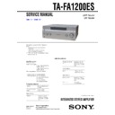
Sony TA-FA1200ES Service Manual ▷ View online
SERVICE MANUAL
INTEGRATED STEREO AMPLIFIER
AEP Model
UK Model
TA-FA1200ES
Ver. 1.1 2006.12
SPECIFICATIONS
9-887-377-02
2006L05-1
© 2006.12
© 2006.12
Sony Corporation
Home Audio Division
Published by Sony Techno Create Corporation
Published by Sony Techno Create Corporation
– Continued on next page –
This amplifier incorporates Dolby* Digital and
DTS**.
*
DTS**.
*
Manufactured under license from Dolby
Laboratories.
“Dolby” and the double-D symbol are
trademarks of Dolby Laboratories.
Laboratories.
“Dolby” and the double-D symbol are
trademarks of Dolby Laboratories.
** “DTS” and “DTS 2.0” are trademarks of Digital
Theater Systems, Inc.
Amplifier section
POWER OUTPUT
Rated Power Output*
8 ohms 1 kHz, THD 0.7%:
110 W + 110 W
4 ohms 1 kHz, THD 0.7%:
120 W + 120 W
110 W + 110 W
4 ohms 1 kHz, THD 0.7%:
120 W + 120 W
Power requirements 230 V AC, 50/60 Hz
* Measured under the following conditions:
Power requirements: 230 V AC, 50/60 Hz
(in countries/area in Europe
other than UK)
240 V AC, 50/60 Hz
(in UK and general area)
other than UK)
240 V AC, 50/60 Hz
(in UK and general area)
Frequency response
Inputs (Analog)
PHONO
RIAA equalization curve
± 0.5 dB
TUNER, SA-CD/CD,
TAPE
TAPE
10 Hz – 40 kHz
± 3 dB (8 ohms)
PHONO
Sensitivity: 2.5 mV
Impedance: 50 kohms
S/N: 86 dB (A, 20 kHz
LPF)
Impedance: 50 kohms
S/N: 86 dB (A, 20 kHz
LPF)
Output (Analog)
Inputs (Digital)
TUNER, SA-CD/CD,
TAPE
TAPE
Sensitivity: 150 mV
Impedance: 50 kohms
S/N: 96 dB (A, 20 kHz
LPF)
Impedance: 50 kohms
S/N: 96 dB (A, 20 kHz
LPF)
TAPE
Voltage: 150 mV
Impedance: 1 kohms
Impedance: 1 kohms
DIGITAL 1/2/3
Impedance: 75 ohms
S/N: 96 dB (A, 20 kHz
LPF)
S/N: 96 dB (A, 20 kHz
LPF)
DIGITAL 4
S/N: 96 dB
(A, 20 kHz LPF)
(A, 20 kHz LPF)
2
TA-FA1200ES
TABLE OF CONTENTS
1.
SERVICING NOTES
................................................
3
2.
GENERAL
...................................................................
7
3.
DISASSEMBLY
3-1.
Disassembly Flow ...........................................................
9
3-2.
Case .................................................................................
9
3-3.
Front Panel Assy .............................................................. 10
3-4.
AC (1) Board ................................................................... 10
3-5.
AC (2) Board ................................................................... 11
3-6.
DC Board ......................................................................... 11
3-7.
Back Panel ....................................................................... 12
3-8.
MAIN DIF Board ............................................................ 13
4.
TEST MODE
.............................................................. 14
5.
DIAGRAMS
5-1.
Block Diagram – CONTROL Section – .......................... 16
5-2.
Block Diagram – DSP Section – ..................................... 17
5-3.
Block Diagram – AMP Section – .................................... 18
5-4.
Block Diagram – POWER SUPPLY Section – ............... 19
5-5.
Schematic Diagram – MAIN DIF Board (1/7) – ............. 21
5-6.
Schematic Diagram – MAIN DIF Board (2/7) – ............. 22
5-7.
Schematic Diagram – MAIN DIF Board (3/7) – ............. 23
5-8.
Schematic Diagram – MAIN DIF Board (4/7)/
PROTECTOR Board – .................................................... 24
PROTECTOR Board – .................................................... 24
5-9.
Schematic Diagram – MAIN DIF Board (5/7) – ............. 25
5-10. Schematic Diagram – MAIN DIF Board (6/7) – ............. 26
5-11. Schematic Diagram – MAIN DIF Board (7/7) – ............. 27
5-12. Printed Wiring Boards
5-11. Schematic Diagram – MAIN DIF Board (7/7) – ............. 27
5-12. Printed Wiring Boards
– MAIN DIF Board (Component Side)/
PROTECTOR Board – .................................................... 28
PROTECTOR Board – .................................................... 28
5-13. Printed Wiring Board
– MAIN DIF Board (Conductor Side) – ......................... 29
5-14. Printed Wiring Board – DSP Board – ............................. 30
5-15. Schematic Diagram – DSP Board – ................................ 31
5-16. Printed Wiring Board – DISPLAY Board – .................... 32
5-17. Schematic Diagram – DISPLAY Board – ....................... 33
5-18. Printed Wiring Boards – PANEL Section – ..................... 34
5-19. Schematic Diagram – PANEL Section – ......................... 35
5-20. Printed Wiring Board – DC Board – ............................... 36
5-21. Printed Wiring Board – AC (2) Board – .......................... 37
5-22. Printed Wiring Board – AC (1) Board – .......................... 38
5-23. Schematic Diagram – POWER SUPPLY Section – ........ 39
6.
EXPLODED VIEWS
6-1.
Case Section .................................................................... 55
6-2.
Display Board Block ....................................................... 56
6-3.
Front Panel Block ............................................................ 57
6-4.
Heat Sink Block ............................................................... 58
6-5.
Transformer Block ........................................................... 59
6-6.
Chassis Block .................................................................. 60
6-7.
Main Board Block ........................................................... 61
7.
ELECTRICAL PARTS LIST
................................ 62
SAFETY-RELATED COMPONENT WARNING!!
COMPONENTS IDENTIFIED BY MARK
0
OR DOTTED LINE
WITH MARK
0
ON THE SCHEMATIC DIAGRAMS AND IN
THE PARTS LIST ARE CRITICAL TO SAFE OPERATION.
REPLACE THESE COMPONENTS WITH SONY PARTS WHOSE
PART NUMBERS APPEAR AS SHOWN IN THIS MANUAL OR
IN SUPPLEMENTS PUBLISHED BY SONY.
REPLACE THESE COMPONENTS WITH SONY PARTS WHOSE
PART NUMBERS APPEAR AS SHOWN IN THIS MANUAL OR
IN SUPPLEMENTS PUBLISHED BY SONY.
Notes on chip component replacement
•
Never reuse a disconnected chip component.
•
Notice that the minus side of a tantalum capacitor may be
damaged by heat.
Output (Digital)
TONE
General
Power requirements 230 V AC, 50/60 Hz
(in countries/area in
Europe other than UK)
240 V AC, 50/60 Hz
(in UK and general area)
Europe other than UK)
240 V AC, 50/60 Hz
(in UK and general area)
Power consumption 100 W
Power consumption (during standby mode)
0.5 W
AC outlets
1 switched, 100 W/0.4 A
Dimensions
430
×
173
×
428 mm
MAX (in countries/area in
Europe other than UK)
Europe other than UK)
including projecting parts
and controls
and controls
Mass (Approx.)
14.0 kg
Supplied accessories
Operating Instructions
Optimizer microphone ECM-AC1 (1)
AC power cord (mains lead) (1)
Remote commander RM-AAU010 (1)
R6 (size-AA) batteries (2)
Design and specifications are subject to
change without notice.
change without notice.
DIGITAL 4
S/N: 96 dB
(A, 20 kHz LPF)
(A, 20 kHz LPF)
TREBLE
±
10 dB, 1 dB step
BASS
±
10 dB, 1 dB step
Ver. 1.1
3
TA-FA1200ES
SECTION 1
SERVICING NOTES
•
MODEL IDENTIFICATION
Model
PART No.
AEP model
2-688-071-1[]
UK model
2-688-072-2[]
UNLEADED SOLDER
Boards requiring use of unleaded solder are printed with the lead-
free mark (LF) indicating the solder contains no lead.
(Caution: Some printed circuit boards may not come printed with
free mark (LF) indicating the solder contains no lead.
(Caution: Some printed circuit boards may not come printed with
the lead free mark due to their particular size)
: LEAD FREE MARK
Unleaded solder has the following characteristics.
• Unleaded solder melts at a temperature about 40 °C higher
than ordinary solder.
Ordinary soldering irons can be used but the iron tip has to be
applied to the solder joint for a slightly longer time.
Soldering irons using a temperature regulator should be set to
about 350
Ordinary soldering irons can be used but the iron tip has to be
applied to the solder joint for a slightly longer time.
Soldering irons using a temperature regulator should be set to
about 350
°C.
Caution: The printed pattern (copper foil) may peel away if
the heated tip is applied for too long, so be careful!
• Strong viscosity
Unleaded solder is more viscou-s (sticky, less prone to flow)
than ordinary solder so use caution not to let solder bridges
occur such as on IC pins, etc.
than ordinary solder so use caution not to let solder bridges
occur such as on IC pins, etc.
• Usable with ordinary solder
It is best to use only unleaded solder but unleaded solder may
also be added to ordinary solder.
also be added to ordinary solder.
NOTE WHEN MEASURING THE VOLTAGE OF THE
CIRCUITS THAT USE VIRTUAL GROUND
CIRCUITS THAT USE VIRTUAL GROUND
This set contains the circuits that take grounding not from usual
ground but from virtual ground.
When measuring circuits in the MAIN DIF board that take “V-GND”
as a ground, take grounding from CNP5202 pin 3 of the MAIN
DIF board.
ground but from virtual ground.
When measuring circuits in the MAIN DIF board that take “V-GND”
as a ground, take grounding from CNP5202 pin 3 of the MAIN
DIF board.
PART No.
– Back Panel –
4
TA-FA1200ES
ERROR MESSAGES
If there is a malfunction, the display shows a code of two numbers and a message. You can check the condition of the system by message.
Refer to the following table to solve the problem.
Refer to the following table to solve the problem.
Messages
Check code
Cause and Response
PROTECTOR
11
Irregular current is output from the speakers. Turn off the ampli-
fier, check the central core of a speaker cord is not touching the
amplifier or other speakers, and turn on again. When using a bi-
wiring connection, check that the metal fittings attached to the
speakers that are used to short the Hi/Lo terminals have been
removed from the speakers.
fier, check the central core of a speaker cord is not touching the
amplifier or other speakers, and turn on again. When using a bi-
wiring connection, check that the metal fittings attached to the
speakers that are used to short the Hi/Lo terminals have been
removed from the speakers.
PROTECTOR
12
The amplifier section is overheated. Check that the ventilation hole
is not covered. Turn off the amplifier, leave the amplifier for a
while, and turn on the power again. When using a bi-wiring
connection, check that the metal fittings attached to the speakers
that are used to short the Hi/Lo terminals have been removed from
the speakers.
is not covered. Turn off the amplifier, leave the amplifier for a
while, and turn on the power again. When using a bi-wiring
connection, check that the metal fittings attached to the speakers
that are used to short the Hi/Lo terminals have been removed from
the speakers.
PROTECTOR
13
The power section is overheated. Check that the ventilation hole is
not covered. Turn off the amplifier, leave the amplifier for a while,
and turn on the power again. When using a bi-wiring connection,
check that the metal fittings attached to the speakers that are used
to short the Hi/Lo terminals have been removed from the speakers.
not covered. Turn off the amplifier, leave the amplifier for a while,
and turn on the power again. When using a bi-wiring connection,
check that the metal fittings attached to the speakers that are used
to short the Hi/Lo terminals have been removed from the speakers.
PROTECTOR
14
Turn off the amplifier, check the central core of a speaker cord is
not touching the amplifier or other speakers.
not touching the amplifier or other speakers.
PROTECTOR
21
Turn off the amplifier and check that the speaker cords are
connected correctly, then turn the power on again. When using a
bi-wiring connection, check that the metal fittings attached to the
speakers that are used to short the Hi/Lo terminals have been
removed from the speakers.
connected correctly, then turn the power on again. When using a
bi-wiring connection, check that the metal fittings attached to the
speakers that are used to short the Hi/Lo terminals have been
removed from the speakers.
Ver. 1.1


