Sharp LC-46XL1E (serv.man5) Service Manual ▷ View online
LC-46XL1E/RU, LC-52XL1E/RU
5 – 29
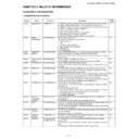
20. IC6281, IC6282: VHILVD104S-1Q
LVDS Receiver
31
PRBS
I
PRBS generator is active when MODE <1:0> = LL (Dual-in/Dual-out mode)
H: PRBS generator is enable. Pattern is PRBS-23.
L: Normal Operation
H: PRBS generator is enable. Pattern is PRBS-23.
L: Normal Operation
10, 11, 12, 16, 28,
32
32
Reserved
I
Must be tied to GND.
23
Reserved
I
Must be Open.
29, 33, 109
N/C
Must be Open.
3, 13, 82, 93, 104,
113, 125, 137
113, 125, 137
VCC
—
Power Supply Pins for TTL inputs, output and digital circuitry.
4, 14, 83, 94, 105,
114, 126, 138
114, 126, 138
GND
—
Ground Pins for TTL inputs, outputs and digital circuitry.
43, 49, 55, 61, 67
LVCC
—
Power Supply Pins for LVDS Outputs.
37, 42, 48, 54, 60,
66, 72
66, 72
LGND
—
Ground Pins for LVDS Outputs.
35, 74
PVCC
—
Power Supply for PLL circuitry.
34, 36, 73, 75
PGND
—
Ground Pin for PLL circuitry.
Pin No.
Pin Name
I/O
Pin Function
LC-46XL1E/RU, LC-52XL1E/RU
5 – 30
Pin No.
Pin Name
I/O
Pin Function
50,49
RA+,RA-
I
LVDS data In.
52,51
RB+,RB-
I
55,54
RC+,RC-
I
60,59
RD+,RD-
I
62,61
RE+,RE-
I
57,56
RCLK+,RCLK-
I
LVDS Clock In.
40, 41, 42, 43,
45, 46, 47
45, 46, 47
RA6-RA0
O
CMOS/TTL Data Outputs.
32, 33, 34, 35,
36, 38, 39
36, 38, 39
RB6-RB0
O
22, 24, 25, 26,
27, 28, 29
27, 28, 29
RC6-RC0
O
14, 15, 17, 18,
19, 20, 21
19, 20, 21
RD6-RD0
O
6, 7, 8, 10, 11, 12,
13
13
RE6-RE0
O
3
PD
I
Power down and Output Control.
H: Normal operation.
L: Power down
H: Normal operation.
L: Power down
4
OE
I
Output Enable.
H: Output enable
L: Output disable.
H: Output enable
L: Output disable.
2
DK
I
Output Clock Delay Timing Select.
tRCP = Output Clock Cycle.
L: Offset 0[nsec]
M: Offset - 3 tRCP (typ) [nsec]
14
H: Offset + 3 tRCP (typ) [nsec]
14
tRCP = Output Clock Cycle.
L: Offset 0[nsec]
M: Offset - 3 tRCP (typ) [nsec]
14
H: Offset + 3 tRCP (typ) [nsec]
14
5
R/F
I
Output Clock Triggering Edge Select.
H: Rising Edge
L: Falling Edge
H: Rising Edge
L: Falling Edge
9, 23, 37, 48
VCC
—
Power Supply Pins for TTL outputs and digital circuitry.
31
CLKOUT
O
Clock out.
1, 16, 30, 44
GND
—
Ground Pins for TTL output and digital circuitry.
53
LVCC
—
Power Supply pin for LVDS inputs.
58
LGND
—
Ground Pin for LVDS inputs.
64
PVCC
—
Power Supply Pin for PLL circuitry.
63
PGND
—
Ground Pin for PLL circuitry.
LC-46XL1E/RU, LC-52XL1E/RU
5 – 31
21. IC6341: RH-iXC029WJQZQ
FPGA
LC-46XL1E/RU, LC-52XL1E/RU
5 – 32
22. IC6342: RH-IXC030WJQZ
PROM
Pin No.
Pin Name
I/O
Pin Function
2
DATA
O
The DATA output signal transfers data selially out of the serial configuration device to the FPGA during
read/configuration operation.
During a read/configuration operations, the serial configuration device is enabled by pulling nCS low.
The DATA signal transitions on the falling edge of DCLK.
read/configuration operation.
During a read/configuration operations, the serial configuration device is enabled by pulling nCS low.
The DATA signal transitions on the falling edge of DCLK.
5
ASDI
I
The AS data input signal is used to transfer data serially into the serial configuration device.
It receives the data that should be programmed into the serial configuration device.
Data is latched in the rising edge of DCLK.
It receives the data that should be programmed into the serial configuration device.
Data is latched in the rising edge of DCLK.
1
nCS
I
The active low chip select input signal toggles at the beginning and end of a valid instruction.
When this signal is high, the device is deselected and the DATA pin is tri_stated.
When this signal is low, it enables the device and puts the device in an active mode.
After power up,the serial configuration device requires a falling edge on the nCS signal before begin-
ning any operation.
When this signal is high, the device is deselected and the DATA pin is tri_stated.
When this signal is low, it enables the device and puts the device in an active mode.
After power up,the serial configuration device requires a falling edge on the nCS signal before begin-
ning any operation.
6
DCLK
I
DCLK is provided by the FPGA.
This signal provides the timing of the serial interface.
The data presented on ASDI is latched to the serial configuration device, at the rising edge of DCLK.
Data on the DATA pin changes after the falling edge of DCLK and is latched into the FPGA on the
rising edge.
This signal provides the timing of the serial interface.
The data presented on ASDI is latched to the serial configuration device, at the rising edge of DCLK.
Data on the DATA pin changes after the falling edge of DCLK and is latched into the FPGA on the
rising edge.
3, 7, 8
VCC
—
Power pins connect to 3.3V.
4
GND
—
Ground pin.

