Sharp LC-32SH130K (serv.man8) Service Manual ▷ View online
49
LC-32SH130E
LC-32SH130K
LC-32SH340E
50
LC-32SH130E
LC-32SH130K
LC-32SH340E
13. SCALER AND LVDS SOCKETS
13.1.
LVDS sockets Block Diagram
13.2.
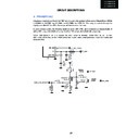
Panel Supply Switch Circuit
This switch is used to open and close panel supply of TCON. It is controlled by port of main μController.
Also with this circuit panel sequence could be adjusted correctly. 3 panel supplies are connected to this
Also with this circuit panel sequence could be adjusted correctly. 3 panel supplies are connected to this
circuit. All of them are optional according to panels.
12.1
12.
12.2
51
LC-32SH130E
LC-32SH130K
LC-32SH340E
52
LC-32SH130E
LC-32SH130K
LC-32SH340E
14. NAND FLASH MEMORY - MX25L1005 (U158)
14.1.
General Description
MX25L1005 is a CMOS 1,048,576 bit serial Flash memory, which is configured as 131,072 x 8 internally.
The MX25L1005 feature a serial peripheral interface and software protocol allowing operation on a simple
3-wire bus. The three bus signals are a clock input (SCLK), a serial data input (SI), and a serial data output
3-wire bus. The three bus signals are a clock input (SCLK), a serial data input (SI), and a serial data output
(SO). SPI access to the device is enabled by CS# input. The MX25L1005 provide sequential read operation
on whole chip. After program/erase command is issued, auto program/ erase algorithms which program/
erase and verify the specified page or sector/block locations will be executed. Program command is
erase and verify the specified page or sector/block locations will be executed. Program command is
executed on page (256 bytes) basis, and erase command is executes on chip or sector(4K-bytes) or
block(64K-bytes). To provide user with ease of interface, a status register is included to indicate the status
block(64K-bytes). To provide user with ease of interface, a status register is included to indicate the status
of the chip. The status read command can be issued to detect completion status of a program or erase
operation via WIP bit. When the device is not in operation and CS# is high, it is put in standby mode and
draws less than 10uA DC current. The MX25L1005 utilize MXIC's proprietary memory cell, which reliably
stores memory contents even after 100,000 program and erase cycles.
14.2.
Features
Serial Peripheral Interface (SPI) compatible -- Mode 0 and Mode 3
1,048,576 x 1 bit structure
32 Equal Sectors with 4K byte each, Any Sector can be erased individually
2 Equal Blocks with 64K byte each, Any Block can be erased individually
Single Power Supply Operation
2.7 to 3.6 volt for read, erase, and program operations
Latch-up protected to 100mA from -1V to Vcc +1V
Low Vcc write inhibit is from 1.5V to 2.5V
14.3.
Absolute Maximum Ratings
RATING
VALUE
Ambient Operating Temperature
0°C to 70°C
Storage Temperature
-55°C to 125°C
Applied Input Voltage
-0.5v to 4.6v
Applied Output Voltage
-0.5v to 4.6v
VCC to Ground Potential
-0.5v to 4.6v
14.4.
Pinning
8-PIN SOP (150mil)
SYMBOL
DESCRIPTION
CS#
Chip select
SI
Serial Data Input
SO
Serial Data Output
SCLK
Clock Input
HOLD#
Hold, to pause the device without
deselecting the device
deselecting the device
VCC
+3.3v Power Supply
GND
Ground
14.4.
Pinning
8-PIN SOP (150mil)
SYMBOL
DESCRIPTION
CS#
Chip select
SI
Serial Data Input
SO
Serial Data Output
SCLK
Clock Input
HOLD#
Hold, to pause the device without
deselecting the device
deselecting the device
VCC
+3.3v Power Supply
GND
Ground
13.
13.3
13.4
13.2
13.1
Click on the first or last page to see other LC-32SH130K (serv.man8) service manuals if exist.

