Sharp LC-32P55E (serv.man40) Service Manual ▷ View online
57
LC-26GA5E
LC-32GA5E
LC-26P55E
LC-32P55E
LC-37P55E
ADVANCE INFORMATION
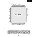
VCT 69xyP
Volume 1: General Description
Micronas
November 3, 2004; 6251-644-1-1
AI
1-65
3.13.Pin Descriptions
3.13.1.Supply Pins
VSUP1.8DIG
− Supply Voltage 1.8 V
This pin is main and standby supply for the digital core
logic of controller, video and display processing.
VSUP1.8FE
− Supply Voltage 1.8 V
This pin is main and standby supply for the analog
video frontend.
VSUP3.3FE
− Supply Voltage 3.3 V
This pin is main and standby supply for the analog
video frontend.
VSUP3.3VO
− Supply Voltage 3.3 V
This pin is main and standby supply for the analog
video outputs.
VSUP1.8LVDS
− Supply Voltage 1.8 V
This pin is main and standby supply for the analog
LVDS core.
VSUP3.3LVDS
− Supply Voltage 3.3 V
This pin is main and standby supply for the Digital
LVDS port.
VSUP3.3FL
− Supply Voltage 3.3 V
This pin is main and standby supply for the Flash
device.
VSUP3.3DRI
− Supply Voltage 3.3 V
This pin is main supply for the digital RAM interface.
VSUP3.3RAM
− Supply Voltage 3.3 V
This pin is main supply for the RAM device
VSUP3.3IO 1-3
− Supply Voltage 3.3 V
This 3 pins are main and standby supply for the digital
I/O-ports.
VSUP3.3COM
− Supply Voltage 3.3 V
This pin is main and standby supply for the digital Input
ports and common digital logic.
VSUP3.3DIG
− Supply Voltage 3.3 V
This pin is main supply for the digital core logic of IF
and audio processing and digital video backend.
VSUP8.0AU
− Supply Voltage 8.0 V
This pin is main supply for the analog audio process-
ing.
VSUP5.0SIF
− Supply Voltage 5.0 V
This pin is main supply for the SIF processing.
VSUP3.3DAC
− Supply Voltage 3.3 V
This pin is main and standby supply for the Analog
DAC.
GND*
− Ground
This pin are main ground for all digital analog and port
supplies.
Application Note:
All GND pins must be connected to a low-resistive
ground plane underneath the IC. All supply pins must
be connected separately with short and low-resistive
lines to the power supply. Decoupling capacitors from
VSUPxx to GND have to be placed as closely as pos-
sible to these pins. It is recommended to use more
than one capacitor. By choosing different values, the
frequency range of active decoupling can be extended.
3.13.2.Audio Pins
VREFAU – Reference Voltage for Analog Audio
This pin serves as the internal ground connection for
the analog audio circuitry. It must be connected to the
GND pin with a 3.3
µF and a 100 nF capacitor in paral-
lel.
SGND
− Analog Reference Input
This is the reference ground Analog Audio part.
AIN1 R/L – Audio 1 Inputs
The analog input signal for audio 1 is fed to this pin.
Analog input connection must be AC coupled.
AIN2 R/L – Audio 2 Inputs
The analog input signal for audio 2 is fed to this pin.
Analog input connection must be AC coupled.
AIN3 R/L – Audio 3 Inputs
The analog input signal for audio 3 is fed to this pin.
Analog input connection must be AC coupled.
AIN4 R/L – Audio 4 Inputs
The analog input signal for audio 4 is fed to this pin.
Analog input connection must be AC coupled.
AIN5 R/L – Audio 5 Inputs
The analog input signal for audio 5 is fed to this pin.
Analog input connection must be AC coupled.
AOUT1 R/L – Audio 1 Outputs
Output of the analog audio 1 signal. Connections to
these pins are intended to be AC coupled.
AOUT2 R/L – Audio 2 Outputs
Output of the analog audio 2 signal. Connections to
these pins are intended to be AC coupled.
SPEAKER R/L – Loudspeaker Outputs
Output of the loudspeaker signal.
HEADPHONES R/L –
H
eadphones Outputs
Output of the headphones signal.
2.2.2. Pin Descriptions
2.2.2.1. Supply Pins
2.2.2.2 Audio Pins
58
LC-26GA5E
LC-32GA5E
LC-26P55E
LC-32P55E
LC-37P55E
VCT 69xyP
ADVANCE INFORMATION
Volume 1: General Description
1-66
November 3, 2004; 6251-644-1-1
AI
Micronas
SUBWOOFER – Subwoofer Outputs
Output of the subwoofer signal
I2S_DEL_WS - Delay Line Bus Word Strobe
This is the word strobe signal of the delay line bus.
I2S_DEL_CL - Delay Line Bus Clock
This is the Clock signal of the delay line bus.
I2S_DEL_IN - Delay Line Bus Data Input
This is the data input signal of the delay line bus.
I2S_DEL_OUT - Delay Line Bus Data Output
This is the data output signal of the delay line bus.
I2S_WS - I2S Word Strobe
This is the word strobe signal of I2S bus.
I2S_DA_IN - I2S Data Input
This is the data input signal of I2S bus.
I2S_CL - I2S Clock
This is the Clock signal of I2S bus.
SPDIF_OUT -
This is an SPDIF output signal to connect to an A/V
receiver.
SIF
−/+ − Sound IF Input
This is the SIF input to connect to an external DRX.
VREFSIF – Reference Voltage for SIF
This pin serves as the internal ground connection for
the analog audio circuitry.
3.13.3.Video Pins
656I 0-7
− Digital 656 Data Input
These are the 8 bits digital 656 video inputs.
656CLKI
− Digital 656 Input clock
This is the clock for the digital 656 video inputs.
656O 0-7
− Digital 656 Data Output
These are the 8 bits digital 656 video outputs.
656CLKO
− Digital 656 output clock
This is the clock for the digital 656 video outputs.
OSDR 0-3
− Graphic Data input/output
These are the 2 or 4 bit graphic input/output
OSDG 0-3
− Graphic Data input/output
These are the 2 or 4 bit graphic input/output
OSDB 0-3
− Graphic Data input/output
These are the 2 or 4 bit graphic input/output
OSDHCS 0-1
− Graphic Half Contrast Input/Output
This is the half contrast for the graphic input/output
OSDFSW
− Graphic Fast Switch Input/Output
This is the fast switch for the graphic input/output
OSDCLK
− Graphic clock Input/Output
This is the clock for the graphic video input/output
OSDV
− Graphic vertical sync Input/Output
This is the vertical sync for the graphic input/output
OSDH
− Graphic horizontal sync Input/Output
This is the horizontal sync signal for the graphic I/O
DRO1_ 0-9 - Digital Red Outputs
This are 10 bits digital signals for red outputs,
for dual RGB use bits (0-7).
DGO1_ 0-9 - Digital Green Output
This are 10 bits digital signals for green outputs,
for dual RGB use bits (0-7).
DBO1_ 0-9 - Digital Blue Outputs
This are 10 bits digital signals for blue outputs,
for dual RGB use bits (0-7).
DRO2_ 0-7 - Digital dual Red Outputs
This are 8 bits digital signals for red outputs.
DGO2_ 0-7 - Digital dual Green Output
This are 8 bits digital signals for green outputs.
DBO2_ 0-7 - Digital dual Blue Outputs
This are 8 bits digital signals for blue outputs.
PCS 0-5 - LCD Panel Control Select Outputs
This are 6 control select signals for LCD outputs.
For CRT application use PCS_0 as H sync and PCS_1
as V sync Back End.
PCLK1,2 - LCD Panel Clock Outputs
This are the clock signals for LCD/RGB outputs.
LVDSA_* - LCD Panel LVDS Outputs
This are 12 signals and clocks for LVDS single or dual
output.
LVDSB_* - LCD Panel LVDS Outputs
This are 10 signals and clocks for LVDS dual output.
REXT - LVDS External Resistor
This pin is connected to the external LVDS resistor.
(6.2 kOhm to gnd)
DRI 0-7 - Digital video inputs for Red
This are 8 bits digital inputs for red signal
DGI 0-7- Digital video inputs for Green
This are 8 bits digital inputs for green signal
DBI 0-7- Digital video inputs for Blue
This are 8 bits digital inputs for blue signal.
2.2.2.3 Video Pins
2.2.2. Pin Descriptions (Continued)
59
LC-26GA5E
LC-32GA5E
LC-26P55E
LC-32P55E
LC-37P55E
ADVANCE INFORMATION
VCT 69xyP
Volume 1: General Description
Micronas
November 3, 2004; 6251-644-1-1
AI
1-67
DEN - Digital video inputs Enable
This is the enable signal for the Digital Video Inputs.
DHS - Digital video inputs Horizontal Sync
This is the H Sync signal for the Digital RGB input bus
or for the VGA Video Inputs.
DVS - Digital video inputs Vertical Sync
This is the V Sync signal for the Digital RGB input bus
or for the VGA Video Inputs.
DCLK - Digital video inputs Clock
This is the Clock signal for the Digital Video Inputs.
CLKOUT
− Digital Output clock
This is a 20MHz clock for the external video ICs.
VIN 1–22
− Analog Video Input
These are the 19 analog video inputs.
(Vin 4,10 and 14 are missing)
A CVBS, S-VHS, YCrCb or RGB signal is converted
using the luma, chroma and component AD converter.
Vin 8,18 are fast blank inputs. Vin22 is an Hsync input.
The input signals must be AC-coupled.
VOUT 1-3
− Analog Video Output
The analog video inputs that are selected by the video
matrix are output at these pins.
ROUT, GOUT, BOUT
− Analog RGB Output
These pins are the analog Red/Green/Blue outputs of
the back-end.
SVMOUT
− Scan Velocity Modulation Output
This output delivers the analog SVM signal. The D/A
converter is a current sink like the RGB D/A convert-
ers. At zero signal the output current is 50% of the
maximum output current.
3.13.4.Controller Pins
XTALIN Crystal Input and XTALOUT Crystal Output
These pins are connected to an 20.25 MHz crystal
oscillator. An external clock can be fed into XTALIN.
RESETQ
− Reset Input/Output
A low level on this pin resets the VCT 69xyP. The
internal CPU can pull down this pin to reset external
devices connected to this pin.
TEST
− Test Input
This pin enables factory test modes. For normal opera-
tion, it must be connected to ground.
SCL
− I
2
C Bus Clock
This pin delivers the I
2
C bus clock line. The signal can
be pulled down by external slave ICs to slow down
data transfer.
SDA
− I
2
C Bus Data
This pin delivers the I
2
C bus data line.
P1_0
−P1_3 − I/O Port
These pins provide CPU controlled I/O ports.
P1_4
−P1_7 − I/O Port
These pins provide CPU controlled I/O ports.
Also used as CADC1
−4 − Controller A/D inputs 1 to 4.
This 4 pins are analog/digital converters from the con-
troller
P2_0
−P2_7 − I/O Port
These pins provide CPU controlled I/O ports.
P3_0
−P3_7 − I/O Port
These pins provide CPU controlled I/O ports.
P4_0
−P4_7 − I/O Port
These pins provide CPU controlled I/O ports.
TDO-TCLK-TDI-TMS -JTAG Interface Pins for TV con-
troler.
TCLK at pin 4 (656O3) has during reset an internal pull
up: (TCLK=0) at end of reset enables the JTAG mode
at 656 LSB’s, this can also be done via I2C.
This JTAG is also available at Port(1 and 2) but only
via I2C.
TDOFW-TCLKFW-TDIFW-TMSFW -JTAG Interface
Pins for firmware controler.
TCLKFW at pin 208 (656O7) has during reset an inter-
nal pull up: (TCLKFW=0) at end of reset enables the
JTAG mode, this can also be done via I2C.
2.2.2.4 Controller Pins
60
LC-26GA5E
LC-32GA5E
LC-26P55E
LC-32P55E
LC-37P55E
VCT 69xyP
ADVANCE INFORMATION
Volume 1: General Description
1-68
November 3, 2004; 6251-644-1-1
AI
Micronas
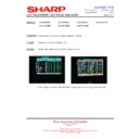
Table 3–10: Maximum Number of Ports
Display
CRT
FPD
Application
Analog RGB + SVMOUT + H + V
TTL (Single RGB),
LVDS (Dual or Single)
TTL (Dual RGB)
Panel
control
X
X
X
X
X
X
X
X
X
X
X
X
656IN
X
X
X
X
X
X
X
X
X
X
X
X
656OUT
X
X
X
X
X
X
X
X
X
X
OSD444
X
X
X
X
X
X
X
X
OSD222
X
X
X
X
Port 1
4
4
4
4
4
4
4
4
8
8
8
8
8
8
8
8
8
8
8
8
Port 2
8
8
8
8
8
8
8
8
6
6
6
6
6
6
6
6
6
6
6
6
Port 3
6
8
8
6
8
8
6
6
8
6
8
8
8
8
Port 4
2
2
2
2
8
8
8
8
8
8
8
8
8
8
Max Number
of Ports
14
20
22
22
20
26
28
28
14
20
20
22
22
28
30
30
14
22
22
30
Note: 24bit RGB input is always available
Maximum Number of Ports


