Sharp LC-28HM2E (serv.man3) Service Manual ▷ View online
61
LC-28HM2
AN-28SP2
6
5
4
3
2
1
A
B
C
D
E
F
G
H
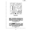
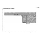
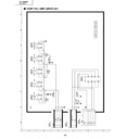
OVERALL WIRING DIAGRAM (AVC SYSTEM)
DUNTKA354NJ01
1
2
3
18
19
20
QCNW-5635CEZZ
(FFC)
PO
WER UNIT
WER UNIT
FR
ONT TERMINAL
ONT TERMINAL
UNIT
MAIN UNIT
REAR TERMINAL
UNIT
PC_GND
1
PC_GND
2
RDENC0322CEZZ
PS-ON
2
2
QCNW-5704CEZZ
1
2
3
18
19
20
1
2
3
20
21
22
DUNTKA352NJ01
50
49
48
3
2
1
1
2
3
28
29
30
50
49
48
3
2
1
QCNW-5632CEZZ
QCNW-5634CEZZ
QCNW-5633CEZZ
(FFC)
(FFC)
(FFC)
1
2
3
48
49
50
30
29
28
3
2
1
1
2
3
28
29
30
DUNTKA353NJ01
QSOCN0487FJZZ*
QSOCN0199FJZZ*
SC2402
SC1403
SC401
QSOCN0464FJZZ*
QSOCN0490FJZZ*
QSOCN0464FJZZ*
QSOCN0464FJZZ*
QPLGN0324FJZZ*
SC1402
SC403
SC402
RXD_M
D_GND
TXD_M
GND
C_CB
C_CR
GND
HP_L
5V(A)
HP_L
5V(A)
GND
V2_PLUG
V2_Y
GND
V2_PLUG
V2_Y
GND
C_CB
C_CR
V3_L
P701
PC_AGND
PC_AGND
PC_AGND
D GND
5V(D)
SMPOW
GND
SRST
FLASH_W
FLASH_W
GND
QSOCN0490FJZZ*
SM_RST
BS_AFCOUT
BS_AFCOUT
BS_DET
BS_BIT
BS_DET
V2_L
5V(A)
5V(A)
BS_BIT
5V(A)
5V(A)
SC1404
V2_R
5V(A)
GND
RXD_M
D_GND
TXD_M
GND
5V(A)
GND
SC404
V3_R
QSOCN0464FJZZ*
62
LC-28HM2
AN-28SP2
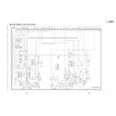
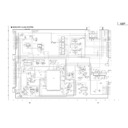
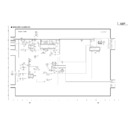
DESCRIPTION OF SCHEMATIC DIAGRAM
VOLTAGE MEASUREMENT CONDITION:
1. When the exclusive-use AC adapter is used, the colour
bar signal of colour bar generator for service is input to
get the normal screen. When the audio is minimized,
the voltage value is measured with the 20 k
get the normal screen. When the audio is minimized,
the voltage value is measured with the 20 k
Ω
/V tester.
WAVEFORM MEASUREMENT CONDITION:
1. When the exclusive-use AC adapter is used, the colour
density, lightness and colour hue are set to the center
position, and the signal of colour bar generator for
service is observed to get waveform.
position, and the signal of colour bar generator for
service is observed to get waveform.
2. indicates waveform check points (See chart,
waveforms are measured from point indicated to
chassis ground.)
chassis ground.)
INDICATION OF RESISTOR & CAPACITOR:
RESISTOR
1. The unit of resistance “
1. The unit of resistance “
Ω
” is omitted.
(K=k
Ω
=1000
Ω
, M=M
Ω
).
2. All resistors are ± 5%, unless otherwise noted.
(J= ± 5%, F= ± 1%, D= ± 0.5%)
3. All resistors are Carbon type, unless otherwise noted.
C
: Solid
W
: Cement
S
: Oxide Film
T
: Special
N
: Metal Coating
CAPACITOR
1. All capacitors are mF, unless otherwise noted.
1. All capacitors are mF, unless otherwise noted.
(P=pF=mmF).
2. All capacitors are Ceramic type, unless otherwise
noted.
(ML) : Mylar
(ML) : Mylar
(TA) : Tantalum
(PF) : Polypro Film
(ST) : Styrol
CAUTION:
This circuit diagram is original one, therefore there may be a
slight difference from yours.
slight difference from yours.
IMPORTANT SAFETY NOTICE:
PARTS MARKED WITH “
å
” ( )ARE
IMPORTANT FOR MAINTAINING THE SAFETY OF
THE SET. BE SURE TO REPLACE THESE PARTS
WITH SPECIFIED ONES FOR MAINTAINING THE
SAFETY AND PERFORMANCE OF THE SET.
THE SET. BE SURE TO REPLACE THESE PARTS
WITH SPECIFIED ONES FOR MAINTAINING THE
SAFETY AND PERFORMANCE OF THE SET.
63
LC-28HM2
AN-28SP2
WAVEFORMS
1
TP7002
V: 500mV/div H: 20µsec/div
2
TP7003
V: 500mV/div H: 20µsec/div
3
TP7004
V: 500mV/div H: 20µsec/div
4
TP7005
V: 500mV/div H: 20µsec/div
5
TP801
V: 500mV/div H: 20µsec/div
6
TP802
V: 500mV/div H: 20µsec/div
7
TP806
V: 500mV/div H: 20µsec/div
8
TP807
V: 500mV/div H: 20µsec/div
9
TP819
V: 500mV/div H: 20µsec/div
0
TP820
V: 500mV/div H: 20µsec/div
q
TP821
V: 500mV/div H: 20µsec/div

