Sharp LL-T1810A (serv.man10) Service Manual ▷ View online
No
Yes
No
Yes
No
Yes
No
Yes
No
Yes
No
Yes
No
Yes
No
Yes
No
Yes
No
Yes
Yes
No
Yes
No
Yes
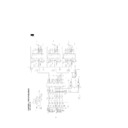
Continued from the preceding page.
IC34 No. 51 pins signal output is at H level
(DC+5V)?
(DC+5V)?
IC34 No. 52 pins signal output is at L level
(0V)?
(0V)?
Check circuits around (LED, cable, etc.).
Check the microprocessor control circuits
around IC29 and IC34.
around IC29 and IC34.
Check the microprocessor control circuits
around IC29 and IC34.
around IC29 and IC34.
< An error occurs in power save mode >
IC34 No. 56 pins signal output is at t L level
(0V)?
(0V)?
Check microprocessor control circuits
around IC28 and IC34.
around IC28 and IC34.
IC34 Nos. 51 and 52 pins signal outputs
show H level (DC+5V)?
show H level (DC+5V)?
Check circuits around LED (operation
board, cable, etc.).
board, cable, etc.).
Check microprocessor control circuits
around IC28 and IC34.
around IC28 and IC34.
< Back light goes out improperly>
No.1 pins of CN1 and CN2 show DC+12V?
Check DC+12V power supply line and
power supply circuit around fuses F1 and F2.
power supply circuit around fuses F1 and F2.
No.4 pins of CN1 and CN2 show DC+5V?
Check inverter board unit and cable.
IC34 No. 55 pins signal output is at the
H level (DC+5V)?
H level (DC+5V)?
Check microprocessor control circuit
around IC29 and IC34.
around IC29 and IC34.
Test terminal TP1 shows DC+11V?
Check DC+11V power supply line (+11V)
and power supply circuit around IC1.
and power supply circuit around IC1.
IC34 No. 54 pins signal output is at the
L level (0V)?
L level (0V)?
No. 5 pins of the CN1 and CN2 show
DC+5V?
DC+5V?
No. 3 pin of CN1 and CN2 shows 0 V when
brightness is maximum (OSD display, BRIGHT 31)?.
brightness is maximum (OSD display, BRIGHT 31)?.
Check circuit around operation board
(operation board, cable, etc.)
(operation board, cable, etc.)
Check inverter board unit.
Check light in LCD module.
Nos. 1 and 2 pins of CN2 on inverter
board unit show approx. 1800 Vrms?
(Use caution to avoid an electrical shock!
Use a high-voltage probe (more than
100:1) for measuring voltage.)
board unit show approx. 1800 Vrms?
(Use caution to avoid an electrical shock!
Use a high-voltage probe (more than
100:1) for measuring voltage.)
Check microprocessor control circuit
around IC29 and IC34.
around IC29 and IC34.
Check DC+11V power supply line (+11V)
and power supply circuit around IC1.
and power supply circuit around IC1.
No
Yes
No
Yes
No
Yes
Yes
No
No
No
No
No
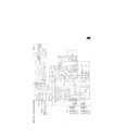
<Screen is not normal >
Test terminal TP3 shows DC+5V?
Check DC+5V power supply line (VCC and
ADVCC) and power supply circuit around IC5.
ADVCC) and power supply circuit around IC5.
IC25 No. 1 pin shows DC+5V?
Check DC+5V power supply line for PLL
and power supply circuit around the IC24.
and power supply circuit around the IC24.
Test terminal TP5 shows DC+3.3V?
Check DC+3.3V power supply line (LVCC)
and power supply circuit around IC7.
and power supply circuit around IC7.
Entire screen of LCD display remains
white?
white?
Signal outputs of clocks FL3, FL4, DE FL2 and FL5
are normal? (See waveform diagrams 6 and 7.)
are normal? (See waveform diagrams 6 and 7.)
Check LCD control signal circuit around
OSC1, OSC2, IC26, IC27 and IC35.
OSC1, OSC2, IC26, IC27 and IC35.
Check LCD connector and LCD module.
Entire screen of LCD display remains
black?
black?
IC34 No. 56 pins signal output is at the
H level (DC+5V)?
H level (DC+5V)?
Check microprocessor control circuit
around IC29 and IC34.
around IC29 and IC34.
No
Yes
Yes
No
Yes
No
No
Check LCD control signal circuit around
IC26 and IC27.
IC26 and IC27.
LCD screen size is abnormal?
Adjustment items of “ADJUSTMENT” and
“MODE SELECT” are set correctly?
“MODE SELECT” are set correctly?
Adjust and set screen according to the
LCD screen setting procedure.
LCD screen setting procedure.
Signal outputs of IC 25 No. 24 pin and IC23 No. 8
pin are normal? (See waveform diagrams 8 and 9.)
pin are normal? (See waveform diagrams 8 and 9.)
Check PLL circuit around IC23, IC25 and
IC34.
IC34.
LCD screen trembles or flickers?
Check PLL circuit around IC23, IC25 and
IC34.
IC34.
Continued on the next page.
Adjust and set screen according to the
LCD screen setting procedure.
LCD screen setting procedure.
Adjustment items of “ADJUSTMENT” and
“MODE SELECT” are set correctly?
“MODE SELECT” are set correctly?
Check LCD control signal circuit around
IC26 and IC27.
IC26 and IC27.
No
Yes
No
No
No
No
No
No
No
Yes
No
No
No
No
Yes
Yes
Yes
Yes
Yes
Yes
Yes
Yes
Yes
Digital color signal inputs and outputs of IC23 and IC27
are normal? (See waveform diagrams 13, 14 and 15.)
are normal? (See waveform diagrams 13, 14 and 15.)
Check color signal processing circuit
around IC23 and IC27.
around IC23 and IC27.
Check microprocessor control circuit
around IC27, IC28 and IC34.
around IC27, IC28 and IC34.
Check the memory circuit around the IC30
and IC34.
and IC34.
Inputs are switched over properly?
IC34 No.3 pins output signal normal?(The signal
is at H level for INPUT1 and at L level for INPUT2.)
is at H level for INPUT1 and at L level for INPUT2.)
Check microprocessor control circuit
around IC14 and IC34.
around IC14 and IC34.
Check Dsub board, cable and CN5, 6.
LCD is normal.
Continued from the preceding page.
LCD screen color is abnormal?
Adjustment items of “GAIN CONTROL” and
“WHITE BALANCE” are set correctly?
“WHITE BALANCE” are set correctly?
Analog color signal outputs of IC 14 Nos. 25, 27, 30 and
35 pins are normal? (See waveform diagrams 10 and 11.)
35 pins are normal? (See waveform diagrams 10 and 11.)
Check video switch circuit around IC14.
Analog color signal outputs of No. 15 pins of IC 401, IC402
and IC403 are normal? (See waveform diagram 12.)
and IC403 are normal? (See waveform diagram 12.)
Check video amplifier circuit around IC401,
IC402, IC403 and IC28.
IC402, IC403 and IC28.
Digital color signal output of IC 23 is
normal? (See waveform diagram 13.)
normal? (See waveform diagram 13.)
Check AD converter circuit around IC23.
Digital color signal input and output of IC 27 is
correct? (See waveform diagrams 14 and 15.)
correct? (See waveform diagrams 14 and 15.)
Check color signal processing circuit
around IC27.
around IC27.
Digital color signal inputs and outputs of
IC8, IC9 and IC10 are normal?
IC8, IC9 and IC10 are normal?
Check color signal processing circuit
around IC8, IC9 and IC0.
around IC8, IC9 and IC0.
Check LCD connector and LCD module
OSD display of LCD screen is abnormal?
Signal outputs of IC31 Nos. 13, 15 and 17
pins are normal? (See waveform diagram 17.)
pins are normal? (See waveform diagram 17.)
Check OSD display circuit around IC31,
IC33 and IC34.
IC33 and IC34.
Check color signal processing circuit
around IC 27.
around IC 27.
LCD screen is normal at composite syn.
and sync.-on-green?
and sync.-on-green?
Check synchronous signal processing circuit
around IC18, IC19, IC21, IC22 and IC38.
around IC18, IC19, IC21, IC22 and IC38.
GAIN CONTROL AUTO operates properly?
Adjust and set screen according to the
LCD screen setting procedure.
LCD screen setting procedure.
Yes
No
Yes
Yes
No
No
No
Yes
No
Yes
No
No
No
No
No
No
No
Yes
No
No
No
No
Yes
Yes
Yes
Yes
Yes
Yes
Yes
Yes
Yes
Digital color signal inputs and outputs of IC23 and IC27
are normal? (See waveform diagrams 13, 14 and 15.)
are normal? (See waveform diagrams 13, 14 and 15.)
Check color signal processing circuit
around IC23 and IC27.
around IC23 and IC27.
Check microprocessor control circuit
around IC27, IC28 and IC34.
around IC27, IC28 and IC34.
Check the memory circuit around the IC30
and IC34.
and IC34.
Inputs are switched over properly?
IC34 No.3 pins output signal normal?(The signal
is at H level for INPUT1 and at L level for INPUT2.)
is at H level for INPUT1 and at L level for INPUT2.)
Check microprocessor control circuit
around IC14 and IC34.
around IC14 and IC34.
Check Dsub board, cable and CN5, 6.
LCD is normal.
Continued from the preceding page.
LCD screen color is abnormal?
Adjustment items of “GAIN CONTROL” and
“WHITE BALANCE” are set correctly?
“WHITE BALANCE” are set correctly?
Analog color signal outputs of IC 14 Nos. 25, 27, 30 and
35 pins are normal? (See waveform diagrams 10 and 11.)
35 pins are normal? (See waveform diagrams 10 and 11.)
Check video switch circuit around IC14.
Analog color signal outputs of No. 15 pins of IC 401, IC402
and IC403 are normal? (See waveform diagram 12.)
and IC403 are normal? (See waveform diagram 12.)
Check video amplifier circuit around IC401,
IC402, IC403 and IC28.
IC402, IC403 and IC28.
Digital color signal output of IC 23 is
normal? (See waveform diagram 13.)
normal? (See waveform diagram 13.)
Check AD converter circuit around IC23.
Digital color signal input and output of IC 27 is
correct? (See waveform diagrams 14 and 15.)
correct? (See waveform diagrams 14 and 15.)
Check color signal processing circuit
around IC27.
around IC27.
Digital color signal inputs and outputs of
IC8, IC9 and IC10 are normal?
IC8, IC9 and IC10 are normal?
Check color signal processing circuit
around IC8, IC9 and IC0.
around IC8, IC9 and IC0.
Check LCD connector and LCD module
OSD display of LCD screen is abnormal?
Signal outputs of IC31 Nos. 13, 15 and 17
pins are normal? (See waveform diagram 17.)
pins are normal? (See waveform diagram 17.)
Check OSD display circuit around IC31,
IC33 and IC34.
IC33 and IC34.
Check color signal processing circuit
around IC 27.
around IC 27.
LCD screen is normal at composite syn.
and sync.-on-green?
and sync.-on-green?
Check synchronous signal processing circuit
around IC18, IC19, IC21, IC22 and IC38.
around IC18, IC19, IC21, IC22 and IC38.
GAIN CONTROL AUTO operates properly?
Adjust and set screen according to the
LCD screen setting procedure.
LCD screen setting procedure.
Yes
No
Yes
Yes
No
No
No
Yes


