Sharp SD-AT50H (serv.man17) Service Manual ▷ View online
SD-AT50H
– 56 –
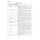
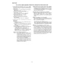
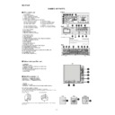
IC507 VHiBA05ST++-1: Switch Regulator (BA05ST)
Terminal Name
Pin No.
Function
1
CTL
Output ON/OFF terminal.
2
VCC
Power supply input terminal.
3
GND
Ground terminal.
4
OUT
Output terminal.
5*
N.C.
For BAOOST/SPF SERIES except for BA00AST/ASTFP, it turns to an N.C. terminal.
In this unit, the terminal with asterisk mark (*) is (open) terminal which is not connected to the outside.
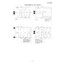
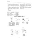
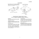
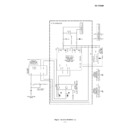
Figure 56-1 BLOCK DIAGRAM OF IC
2
4
1
3
VCC
OUT
CTL
GND
REFFERENCE
VOLTAGE
Figure 56-2 BLOCK DIAGRAM OF IC
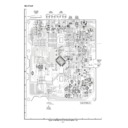
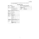
IC701 RH-iX0564AWZZ: System Microcomputer (IX0564AW)
1
2
3
4
5
6
7
8
24
23
22
21
20
19
18
17
9
10 11 12 13 14 15 16
32 31 30 29 28 27 26 25
A/D_REST
N.C.
SP_RLY
BASS_SW
AC_DETECT
AMP_CLK
AMP_SOUT
RESET
CNVSS
XIN
VSS
VDD
VDDE
AMP_INT
POWER_ON
+B_CHECK
PROTECT
FAN_CHK
FAN_LOCK
F_S_MUTE
C_S_MUTE
S_S_MUTE
W_S_MUTE
AMP_STB
SYS_STOP
OFF_SET
UNSW_CHK
POWER
-B_CONT
XOUT
AMP_SIN
D3
D4
D5
D6/CNTR0
D7/CNTR1
P20/SCK
P21/SOUT
P22/SIN
REST
CNVSS
XOUT
XIN
VSS
VDD
VCE
P30/INT0
P31/INT1
AIN0/CMP0-
AIN1/CMP0+
AIN2/CMP1-
AIN3/CMP1+
P00
P01
P04
P03
P10
P11
P12
P13
D0
D1
D2
IC701
IX0564AW
– 57 –
SD-AT50H
IC701 RH-iX0564AWZZ: System Microcomputer (IX0564AW)
1
D3
A/D_RESET
Output
Output of 1 bit AMP
∆∑
IC reset control.
“H” output : normal operation, reset when switching from “L” to “H”.
2*
D4
N.C.
Output
Open terminal. “L” is output, PWB is open.
3
D5
SP_RLY
Output
Speaker relay output. (For all the speakers)
“H” output : relay ON, electric conduction, “L” output : relay OFF
“H” output : relay ON, electric conduction, “L” output : relay OFF
4
D6/CNTR0
BASS_SW
Output
Output for controlling the gain of SUBWOOFER amp.
“H” output : BASS OFF, “L” output : BASS ON
“H” output : BASS OFF, “L” output : BASS ON
5
D7/CNTR1
AC_DETECT
Input
Power failure check with the voltage after the AC rectification.
Normal : “L”, power failure detection when switching from “L” to “H”.
Normal : “L”, power failure detection when switching from “L” to “H”.
6
P20/SCK
AMP_CLK
Input
Clock input for communication with the system microcomputer.
Serial auto send/receive.
Serial auto send/receive.
7
P21/SOUT
AMP_SIN
Output
Data output to the system microcomputer. Serial auto send/receive.
8
P22/SIN
AMP_SOUT
Input
Data input from the system microcomputer. Serial auto send/receive.
9
RESET
RESET
Input
Reset input for this microcomputer. Active “L”.
10
CNVSS
CNVSS
Input
0 V (GND).
11
XOUT
XOUT
Output
Reference oscillation output for this microcomputer.
2 MHz ceralcok connection.
2 MHz ceralcok connection.
12
XIN
XIN
Input
Reference oscillation input for this microcomputer.
2 MHz ceralcok connection.
2 MHz ceralcok connection.
13
VSS
VSS
Input
GND terminal.
14
VDD
VDD
Input
Positive power supply terminal.
15
VDCE
VDCE
Input
Control of the operation and stop of voltage drop detect circuit.
Used in the stop status (connected to GND).
Used in the stop status (connected to GND).
16
P30/INT0
AMP_INT
Output
Communication request signal to the system microcomputer.
Request when switching from “H” to “L”.
Request when switching from “H” to “L”.
17
P31/INT1
POWER_ON
Input
SW input for POWER ON/OFF test mode.
“H” : normal status, “L” : TEST mode ON/OFF
“H” : normal status, “L” : TEST mode ON/OFF
18
AIN0/CMP0-
+B_CHECK
Input
Power rise monitoring input.
Decision of the reset timing of 1 bit AMP.
Decision of the reset timing of 1 bit AMP.
19
AIN1/CMP0+
PROTECT
Input
A/D import, system abnormality detect input.
20
AIN2/CMP1-
FAN_CHK
Input
A/D import, FAN motor rotation detect input.
21
AIN3/CMP1+
FAN_LOCK
Input
A/D import, FAN motor lock detect input.
22
P00
F_S_MUTE
Output
Front speaker S-MUTE output.
“H” output : MUTE-ON, “L” output : MUTE-OFF.
“H” output : MUTE-ON, “L” output : MUTE-OFF.
23
P01
C_S_MUTE
Output
Center speaker S-MUTE output.
“H” output : MUTE-ON, “L” output : MUTE-OFF.
“H” output : MUTE-ON, “L” output : MUTE-OFF.
24
P02
S_S_MUTE
Output
Surround speaker S-MUTE output.
“H” output : MUTE-ON, “L” output : MUTE-OFF.
“H” output : MUTE-ON, “L” output : MUTE-OFF.
25
P03
W_S_MUTE
Output
Subwoofer speaker S-MUTE output.
“H” output : MUTE-ON, “L” output : MUTE-OFF.
“H” output : MUTE-ON, “L” output : MUTE-OFF.
26
P10
AMP_STB
Input
Communication request signal from the system microcomputer.
Request when switching from “H” to “L”.
Request when switching from “H” to “L”.
27
P11
—
Input
PULL_UP
28
P12
SYS_STOP
Input
Power failure detect input. This microcomputer switches to the backup mode.
Normal : “H”, power failure detection when switching from “H” to “L”.
Normal : “H”, power failure detection when switching from “H” to “L”.
29
P13
OFF_SET
Input
Abnormality detection output of 1 bit AMP
∆∑
IC output offset voltage.
L : abnormal
30
D0
UNSW_CHK
Input
Power rise timing control. The power is not risen in “L”.
31
D1
POWER
Output
Output of power supply control.
“L” output : POWER ON, “H” output : POWER OFF.
“L” output : POWER ON, “H” output : POWER OFF.
32
D2
-B_CONT
Output
Control output for - B power supply control relay of 1 bit AMP section.
“L” output : relay ON, -B supply “H” output : relay OFF
“L” output : relay ON, -B supply “H” output : relay OFF
Terminal Name
Pin No.
Input/Output
Function
In this unit, the terminal with asterisk mark (*) is (open) terminal which is not connected to the outside.
Port Name
SD-AT50H
– 58 –
1
VDDL
Input
L channel digital output section power terminal
2
OUTL (+)
Output
L channel forward output terminal
3
OUTL (–)
Output
L channel reverse output terminal
4
GNDD
—
Digital output section ground terminal
5
OUTR (–)
Output
R channel reverse output terminal
6
OUTR (+)
Output
R channel forward output terminal
7
VDDR
Input
R channel digital output section power terminal
8
VDDX
Input
Oscillation section power terminal
9
XI
Input
Quartz oscillator connection terminal. Clock necessary for the system is generated.
10
XO
Output
Quartz oscillator connection terminal. Clock necessary for the system is generated.
11
GNDX
—
Oscillation section ground terminal
12
MCK
Output
System clock output terminal
13
TEST
Input
Test terminal. As usual, it is used at "L".
14
NFR1 (+)
Input
R channel forward signal feedback input terminal
15
NFR2 (–)
Input
R channel reverse signal feedback input terminal
16
GNDA
—
Analog ground terminal for AD converter
17
Rch IN
Input
R channel analog input terminal
18
Rch Vref
Input
Reference voltage terminal for R channel
19
Lch Vref
Input
Reference voltage terminal for L channel
20
Lch IN
Input
L channel analog input terminal
21
RESET
Input
Reset terminal. It is reset with "L".
22
NFL2 (–)
Input
L channel reverse signal feedback input terminal
23
NFL1 (+)
Input
L channel forward signal feedback input terminal
24
VDDA
Input
Analog current terminal for AD converter
Pin No.
Port Name
Input/Output
Function
ICA100, ICA200, ICA300 RH-iX2815AFZZ: 7th Order Modulation Conversion LSI (IX2815AF)
1
2
3
4
5
6
7
8
9
10
11
12
24
23
22
21
20
19
18
17
16
15
14
13
VDDL
VDDA
NFL1(+)
NFL2(–)
RESET
Lch IN
Lch Vref
Rch Vref
Rch IN
GNDA
NFR2(–)
NFR1(+)
TEST
OUTL(+)
OUTL(–)
GNDD
OUTR(–)
OUTR(+)
VDDR
VDDX
XI
XO
GNDX
MCK
1
2
3
4
5
6
7
8
9
10
11
12
24
23
22
21
20
19
18
17
16
15
14
13
VDA
NFL1(+)
NFL2(–)
RESET
Lch IN
Lch Vref
Rch Vref
Rch IN
GNDA
NFR2(–)
NFR1(+)
TEST
VDDL
OUTL(+)
OUTL(–)
GNDD
OUTR(–)
OUTR(+)
VDDR
VDDX
XI
XO
GNDX
MCK
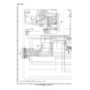
Comparator
Comparator
Amplitude Doubling
Converter
Amplitude Doubling
Converter
Oscillator
Lch 7th order
Modulation Circuit
Rch 7th order
Modulation Circuit
Figure 58 BLOCK DIAGRAM OF IC
– 59 –
SD-AT50H
ICA102, ICA107, ICA202, ICA207, ICA302, ICA307
VHiSLA5505M-1: Switching Audio Power Amp. (SLA5505M)
VHiSLA5505M-1: Switching Audio Power Amp. (SLA5505M)
Figure 59 BLOCK DIAGRAM OF IC
HINA
HINB
Level
Shift
Down
Level
Shift
Down
LS
LS
L/S
L/S
H/S
H/S
CS
CS
LINA
LINB
GND
VKK
V
DD
V
CC
VBBA
VBBB
VBOOTB
VBOOTA
OUTA
OUTB
SA
SB
-Vbb
+Vbb
L
P
F
P
F
L
P
F
P
F

