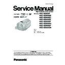
Panasonic HDC-SD600P / HDC-SD600EB / HDC-SD600EC / HDC-SD600EEK / HDC-SD600EF / HDC-SD600EG / HDC-SD600EP / HDC-SD600GN Service Manual ▷ View online
41
10.2. What Is The Factory Settings?
The factory settings clean up and/or refresh the following settings.
1. MENU, MODE, ADJUSTMENT VALUE.
2. SD card format.
3. Reset the folder number and file number of still pictures.
2. SD card format.
3. Reset the folder number and file number of still pictures.
(Setting the folder number is 100, and file number is 0.)
4. Clear the mechanism lock information.
5. Clear the service mode information contents.
6. Close the lens cover
7. Initialize the VIERA Link Physical Address.
5. Clear the service mode information contents.
6. Close the lens cover
7. Initialize the VIERA Link Physical Address.
The setting position of factory settings:
Name
Setting position
Mode switch
Motion picture recording mode
S-1
S1. About Indication of The Schematic Diagram ............................ S-1
S1.1. Important Safety Notice......................................................... S-1
S2. Voltage Chart ........................................................................... S-2
S2.1. Strobe P.C.B. ......................................................................... S-2
S2.2. BATT_Catcher P.C.B. ............................................................ S-2
S2.3. Front P.C.B. ........................................................................... S-2
S2.4. MIC AMP P.C.B. .................................................................... S-2
S3. Block Diagram .......................................................................... S-3
S3.1. Overall Block Diagram .......................................................... S-3
S4. Schematic Diagram .................................................................. S-4
S4.1. Interconnection Diagram ....................................................... S-4
S4.2. Strobe Schematic Diagram ................................................... S-5
S4.3. BATT_Catcher Schematic Diagram ...................................... S-6
S4.4. Front Schematic Diagram ..................................................... S-7
S4.5. MIC AMP Schematic Diagram ............................................... S-8
S4.6. Side R Schematic Diagram ................................................... S-9
S4.7. SS SW Schematic Diagram .................................................. S-9
S4.8. Monitor Schematic Diagram ................................................ S-10
S4.9. MIC AMP FPC Schematic Diagram .................................... S-11
S5. Print Circuit Board .................................................................. S-12
S5.1. Strobe P.C.B. ....................................................................... S-12
S5.2. BATT_Catcher P.C.B. .......................................................... S-13
S5.3. Front P.C.B. ......................................................................... S-14
S5.4. MIC AMP P.C.B. .................................................................. S-15
S5.5. Side R P.C.B. ...................................................................... S-16
S5.6. SS SW P.C.B. ...................................................................... S-16
S5.7. Monitor P.C.B. ..................................................................... S-17
S5.7.1. Monitor P.C.B. (Component Side) .................................... S-17
S5.7.2. Monitor P.C.B. (Foil Side) ................................................. S-18
S5.8. MIC AMP FPC P.C.B. .......................................................... S-19
S6. Replacement Parts List .......................................................... S-21
S7. Exploded View ....................................................................... S-29
S7.1. Frame and Casing Section (1) ............................................ S-29
S7.2. Frame and Casing Section (2) ............................................ S-30
S7.3. LCD Section ........................................................................ S-31
S7.4. Camera Lens Section.......................................................... S-32
S7.5. Packing Parts and Accessories Section .............................. S-33
Table of contents
Service Manual
VM1005029CE
Diagrams and Replacement
Parts List
Vol. 1
Colour
(K)...........Black Type
(H)...........Glay Type (only EB)
Model No.
HDC-SD600P
HDC-SD600EB
HDC-SD600EC
HDC-SD600EE
HDC-SD600EF
HDC-SD600EG
HDC-SD600EP
HDC-SD600GN
High Definition Video Camera
Name of Signal
OFTR
FEP
This signal is connected
to the FEP schematic diagram.
Circuit name being connected.
6.Use the parts number indicated on the Replacement Parts List .
7.Indication on Schematic diagrams:
7.Indication on Schematic diagrams:
5.The voltage being indicated here may be include observational-error (deviation) due to
internal-resistance and/or reactance of equipment. Therefore, handle the value
indicated on here as reference.
4.Although the voltage and waveform available on here is measured with standard frame,
it may be differ from actual measurement due to modification of circuit and so on.
3.The voltage being indicated on the schematic diagram is measured in
"Standard-Playback" mode when there is no specify mode is mentioned.
2.It is only the "Test Round" and no terminal (Pin) is available on the P.C.B.
when the TP (Test Point) indicated as " " mark.
1.Although reference number of the parts is indicated on the P.C.B. drawing and/or
schematic diagrams, it is NOT mounted on the P.C.B. when it is displayed with "$" mark.
FOR SAFETY. WHEN REPLACING ANY OF THESE COMPONENTS USE ONLY THE SAME TYPE.
COMPONENTS IDENTIFIED WITH THE MARK
HAVE THE SPECIAL CHARACTERISTICS
S1. About Indication of The Schematic Diagram
S1.1. Important Safety Notice
S-2
S2. Voltage Chart
S2.1. Strobe P.C.B.
Note) Indicated voltage values are the standard values for the unit measured by the DC electronic circuit tester (high-impedance) with the chassis taken as standard.
Therefore, there may exist some errors in the voltage values, depending on the internal impedance of the DC circuit tester.
REF No.
PIN No. POWER ON
IC7001
1
0
IC7001
2
0
IC7001
3
0
IC7001
4
0
IC7001
5
3.3
IC7001
6
0
IC7001
7
0
IC7001
8
0
IC7001
9
2.9
IC7001
10
8.3
Q3901
E
3.3
Q3901
C
3.3
Q3901
B
3.3
S2.2. BATT_Catcher P.C.B.
REF No.
PIN No. POWER ON
IC6302
1
3.2
IC6302
2
0
IC6302
3
0
IC6302
4
2.9
IC6302
5
3.2
S2.3. Front P.C.B.
REF No.
PIN No. POWER ON
Q6401
E
5.1
Q6401
C
-0.4
Q6401
B
5.1
QR6401
E
0
QR6401
C
4.8
QR6401
B
0
S2.4. MIC AMP P.C.B.
REF No.
PIN No. POWER ON
IC4803
1
2.5
IC4803
2
2.5
IC4803
3
2.5
IC4803
4
0
IC4803
5
2.5
IC4803
6
2.5
IC4803
7
2.5
IC4803
8
4.8
Q4801
E
4.1
Q4801
C
4.8
Q4801
B
4.8
S-3
S3. Block Diagram
S3.1. Overall Block Diagram
IRIS/
ND
LENS(F1.5-2.8 12x)
IC701
LENS/OIS DRIVE
IC2010
CONFIRM
SYSTEM
IC7001
FLASH CHARGE
CONTROL
SD
CARD
USB TERMINAL
SPEAKER
ECM
OPERATION
DC IN
BATTERY
FLASH
REMOTE
SENSOR
S
H
U
TT
E
R
IC4803
MIC AMP
MIC AMP
HDC-SD600 OVERALL BLOCK DIAGRAM
IC151
MOS IMAGE
SENSOR x 3
IC3403
PLL
A/V
MULTI
TERMINAL
HDMI mini
CONNECTOR
X301
OSC
(60MHz)
ZOOM/
FOCUS
MOTOR/
OIS
Analog
Analog
Analog
Analog
Analog
Analog
IC6301
GYRO
SENSOR
CLK13M
CLK74M
CLK12M
IC3402
NAND
FLASH ROM/
512Mbit
COLOR LCD
PANEL
IC3401
MPEG CODEC
(UNI PHIER XP2)
IC3701
AVIO
IC2006
SYSTEM CONTROL
(CAMERA MICROCOMPUTER)
IC1001
POWER CIRCUIT
IC2304
RTC
IC2002
EEPROM
NOTE
: VIDEO SIGNAL
: AUDIO SIGNAL
: CLK or CONTROL LINE
IC301
CAMERA DSP
(BIANCA)
X2301
(32.768kHz)
IC3801
HDMI
LSI
B6401
Li-BATT
Click on the first or last page to see other HDC-SD600P / HDC-SD600EB / HDC-SD600EC / HDC-SD600EEK / HDC-SD600EF / HDC-SD600EG / HDC-SD600EP / HDC-SD600GN service manuals if exist.

