Sharp VC-M314 (serv.man2) Service Manual ▷ View online
55
VC-M314HM
VC-MH834HM
VC-MH834HM
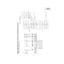
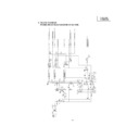
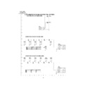
FLOW CHART NO.28 DECODER TROUBLESHOOTING (For 2 SCART Hi-Fi and MONO model)
SELECT
OUTPUT
INPUT
SIGNAL
OUTPUT
SIGNAL
<Hi-Fi
Audio Double scart>
MODE
SIG.
DECODER CIRCUIT
SIG.
FLOW
INPUT
FLOW
(A)
Pin47 of IC701(Y/C video output
E2(L2) video input
Front video input
pin7
pin28
pin25
E1(L1) video output
21PIN CONNECT
OR
(B)
(C)
pin13
pin2
E1(L1) audio output (L-ch)
(A)
(B)
E2(L2) audio input(L/R-ch)
Pin56 of IC6301(Audio output R-ch)
pin33
pin1
1
pin1 E1(L1) audio output(R-ch)
pin42
21PIN CONNECT
OR
(C)
(A)
(B)
E2(L2) audio intput(R-ch)
pin34
pin10
pin18 E2(L2) video output(L-ch)
pin43
21PIN CONNECT
OR
(C)
(A)
(B)
E1(L1) video input
Pin47 of IC701(Y/C video output)
pin23
pin7
pin16
pin26
21PIN CONNECT
OR
(C)
(A)
(B)
E1(L1) audio input(L-ch)
pin36
pin2
pin15
pin30
(C)
(A)
(B)
pin37
(
C)
pin1
(A) E2(L2) video input
pin28
(B) E1(L1) video input
pin23
(C)
T
uner video output
pin18
(D)
pin13
(A) E2(L2) audio input(L-ch)
pin33
(B) E1(L1) audio input(L-ch)
pin36
(C) MPX output(L-ch)
pin16
(D)
pin1
1
(A) E2(L2) audio input (R-ch)
pin34
(B) E1(L1) audio input (R-ch)
pin37
(C)
pin15
(D)
pin10
NO
NO
NO
YES
YES
YES
Check STBY
5V line.
Check STBY
12V line.
Check line between pins(21), (22)
of IC2501 and pins(17), (18) of
IC701.
Is there SDA
and SCL
signal
applied to pins(21) and (22) of
IC2501?
Is voltage 5V applied to the video
section power terminal at pins(24),
(29) of IC2501?
Is voltage 12V applied to the
audio section power terminal at
pins(14) of IC2501?
Check signal line from video and
audio function logic table as shown
below
.
Not output from 21pin connector in video and audio signal.
<Linear
Audio Double scart>
MODE
SIG.
DECODER CIRCUIT
SELECT
INPUT
SIGNAL
FLOW
SIG.
FLOW
INPUT
OUTPUT
OUTPUT
SIGNAL
Pin47 of IC701(Y/C video output)
E2(L2) video input
Front video input
pin7
pin28
pin25
E1(L1) video output
21PIN CONNECT
OR
(B)
(C)
Pin1
1 of IC201 (Audio output)
I
Front audio input
pin13
pin2 pin 42
E1(L1) audio output(L/R
(A)
E2(L2) audio input(L/R-ch)
pin33
pin1
1
-ch)21PIN CONNECT
OR
(C)
(A)
E1(L1) video input
Pin47 of IC701(Y/C video output)
pin18
pin23
pin7
pin26
E2(L2) video output
21PIN CONNECT
OR
(B)
(C)
(A)
E1(L1) audio input(L/R-ch)
Pin1
1 of IC201(Audio output)
pin16
pin36
pin2
pin30
E2(L2) audio output(L/R
-ch)21PIN CONNECT
OR
(B)
(C)
(A)
E1(L1) video input
pin28
pin23
pin18
pin5
Pin31 of IC201
Y/C video input
(Aux. input)
(B)
(C)
(D)
E2(L2) audio input (L/R-ch)
E1(L1) audio input(L/R-ch)
Front audio input
pin13
pin33
pin36
(A)
(B)
(C)
pin16
pin1
1
pin39
Pin 9 of IC201
Audio input
(D)
T
uner video output
Front video input
Pin58 of IC6301(Audio output L-ch)
T
uner video output
MPX output(L-ch)
Pin58 of IC6301(Audio output(L-ch))
21PIN CONNECT
OR
E2(L2) audio output (L-ch)
pin31
E2(L2) audio output (R-ch)
21PIN CONNECT
OR
Pin31 of IC201
Y/C video input
(Aux. input)
Pin61 of IC6301
(Aux. input
Pin52 of IC6301
(Audio input (R-ch)
pin5
pin39
pin40
Front audio L-ch input
Front audio R-ch input
Front audio L-ch input
Front audio R-ch input
MPX output (R-ch)
>
>
>
>
>
>
>
>
>
>
>
>
>
>
>
>
>
>
>
>
>
>
>
>
>
>
>
>
>
>
>
>
>
>
>
>
>
>
>
>
>
>
>
>
>
>
>
>
>
>
>
>
>
>
>
>
>
>
>
>
>
>
>
>
>
MPX output(R-ch)
Front video input
(A)
(B)
T
uner video output
T
uner audio output
E2(L2) video input
T
uner audio output
(switch)
(switch)
E1(L1) audio input(R-ch)
Pin56 of IC6301(Audio output R-ch)
56
VC-M314HM
VC-MH834HM
VC-MH834HM
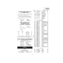
REPLACEMENT OF IC705(E
2
PROM)
Servicing precautions
When the IC705(E
2
PROM) has been replaced, make the following reprogramming.
Depending on models, the IC705(E
2
PROM) has been factory adjusted for it’s memory function.
It’s therefore necessary to reprogram the memory function for the model in question.
Note that the servo circuit requires readjustments for the slow and still modes.
Note that the servo circuit requires readjustments for the slow and still modes.
1. Memory function reprogramming.
a. Check the power off.(Power is standby mode)
b. Make for moment short-circuit test point(P802), located at the front side on the main PWB.
b. Make for moment short-circuit test point(P802), located at the front side on the main PWB.
Be sure that all the display light up into the TEST mode.
c. Using the CHANNEL(+) AND (–) buttons, select the right function numbers from JP0 to JP39, which appear in the
display, referring to the E
2
PROM map.
Press the DISPLAY button to pickup the functions(ON) and the CLEAR button to discard the functions(OFF).
DISPLAY and CLEAR buttons, are located on the remote control unit.
DISPLAY and CLEAR buttons, are located on the remote control unit.
∗
when the DISPLAY button has been pressed (ON), the memory function number starts flashing.
∗
when the CLEAR button has been pressed (OFF), the memory function number lights up.
d. Example : "ON" and "OFF" are taken as "1" and "0" respectively.
The numbers JP0 to JP39 are divided into four groups and each group’s setting is displayed in hexadecimal notation.
JP27 JP26 JP25 JP24
1
1
0
0
↓
C
JP23 JP22 JP21 JP20
0
0
0
0
↓
0
JP19 JP18 JP17 JP16
0
0
0
0
↓
0
JP15 JP14 JP13 JP12
0
1
0
0
↓
4
JP11 JP10 JP9 JP8
0
0
1
1
↓
3
JP7 JP6 JP5 JP4
0
0
0
0
↓
0
JP3 JP2 JP1 JP0
0
0
0
0
↓
0
Also recording level preset number selected from the ten keys on the remote control unit which appear in the
LCD display, referring to the E
LCD display, referring to the E
2
PROM map.
JP39 JP38 JP37 JP36
0
0
0
0
↓
0
JP35 JP34 JP33 JP32
0
0
0
1
↓
1
JP31 JP30 JP29 JP28
0
0
0
0
↓
0
SP n
∗
∗
↑
selection from the
ten keys.
(from "0" to "7")
ten keys.
(from "0" to "7")
EP n
∗
∗
↑
selection from the
ten keys.
(from "0" to "7")
ten keys.
(from "0" to "7")
Out lights
blank
SP p
∗
∗
↑
selection from the
ten keys.
(from "0" to "7")
ten keys.
(from "0" to "7")
LP p
∗
∗
↑
selection from the
ten keys.
(from "0" to "7")
ten keys.
(from "0" to "7")
2. Memory recording preset level reprogramming.
a. Similarly to the above step 1-a and 1-b the same operate.
b. Using the CHANNEL (+) AND (-) buttons, select the right function numbers continued from recording preset number
b. Using the CHANNEL (+) AND (-) buttons, select the right function numbers continued from recording preset number
as has been JP0~JP39, which appear in the LCD display, referring to the E
2
PROM map.
3. Example :
System
p : PAL
n : NTSC
n : NTSC
↓
Tape speed
→
LP or EP
n
∗
∗
↑
↑
Chrominance preset number. (from "0" to "7")
Luminance preset number. (from "0" to "7")
3. Finally make for a moment short-circuit test point(P802), both located at the front side on the main PWB to clear the
TEST mode.
↑
↑
↑
↑
57
VC-M314HM
VC-MH834HM
VC-MH834HM
4. Jumper setting of JP0 to JP39 in hexadecimal notation and REC current setting.
d. Example:
c. The jumper setting in hexadecimal notation and REC current setting will be displayed on the
television screen (upper left).
television screen (upper left).
a. Check the power on. (Power is ON)
b. Make short circuit test point(P802) and hold the point.
Be sure that all the LCD display light up into the TEST mode.
b. Make short circuit test point(P802) and hold the point.
Be sure that all the LCD display light up into the TEST mode.
YC 44220707
VM F8F9
NOR--
VM F8F9
NOR--
If the jumper setting is set as step 1-d, it will be displayed on television screen
like the example above.
like the example above.
5. Finally release the test point to return to normal screen (E-E mode).
YC 4 4 2 2 0 7 0 7
V
V V
V
SP LP
SP
EP
PAL
NTSC
V
V
V
JP 003400C010
58
VC-M314HM
VC-MH834HM
VC-MH834HM
ROM MAP
MODEL
MH834HM
M314HM
PAL SP
44
34
PAL LP
22
34
SECAM SP
07
07
SECAM LP
07
07
IC701
iX1669GE
iX1673GE
JP39
A.DUB
0
0
JP38
NOT SLOW ATR
0
1
JP37
S.SIMPLE PB
1
0
JP36
NTPB
1
0
JP35
NTSC SKEW
0
0
JP34
HEAD 2
0
0
JP33
HEAD 1
1
0
JP32
HEAD 0
0
1
JP31
GAMMA
0
0
JP30
SAT CTL BUILT IN
0
0
JP29
POSI84
1
0
JP28
R/C CODE
0
0
JP27
DNR
0
0
JP26
POST CODE
1
0
JP25
SAT CTL
1
0
JP24
AV LINK/16:9
1
0
JP23
Hi-Fi
1
0
JP22
SORT/CLOCK
1
0
JP21
DECODER
1
0
JP20
SURROUND
0
0
JP19
IGR
0
0
JP18
NICAM
1
0
JP17
G-CODE1
1
1
JP16
G-CODE0
1
1
JP15
EP
1
0
JP14
LP
0
1
JP13
F-AV
1
0
JP12
2 SCART
1
0
JP11
RF OUTPUT OFF
0
0
JP10
TUNER2
0
0
JP9
TUNER1
1
1
JP8
TUNER0
1
1
JP7
SYSTEM1
0
0
JP6
SYSREM0
0
0
JP5
380FF/REW
1
0
JP4
LOW POWER
0
0
JP3
OEM
0
0
JP2
VPS/PDC
1
0
JP1
COLOUR1
0
0
JP0
COLOUR0
0
0
DISPLAY
3227E7B324
4100034300
0:LIGHT UP
1:FLASHING

