Sharp TU-X1E (serv.man8) Service Manual ▷ View online
TU-X1E/RU
7 – 21
[4] TUNER UNIT
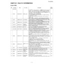
1. VHIDRX3913K-1Y Multi Standard Demodulator
Pin No.
Pin Name
I/O
Pin Function
1
I2S_WS
I
I2S Word Strobe
2
VDDL
-
Digital Core Supply 1.2V
3
VSSL
-
Digital Core GND
4
GPIO1
I/O
User Programmable IO-1
5
MSTRT
I
MPEG Start
6
MERR
I
MPEG Error
7
VSSH
-
Digital IO GND
8
VDDH
-
Digital IO Supply 3.3V
9
MCLK
I
MPEG Clock
10
MVAL
I
MPEG Valid
11
MD0
I
MPEG Data[0]
12
MD1
I
MPEG Data[1]
13
MD2
I
MPEG Data[2]
14
MD3
I
MPEG Data[3]
15
VSSL
-
Digital Core GND
16
VDDL
-
Digital Core Supply 1.2V
17
VSSH
-
Digital IO GND
18
VDDH
-
Digital IO Supply 3.3V
19
MD4
I
MPEG Data[4]
20
MD5
I
MPEG Data[5]
21
MD6
I
MPEG Data[6]
22
MD7
I
MPEG Data[7]
23
I2C_SCL1
I
Primary I2C interface Clock
24
I2C_SDA1
I/O
Primary I2C interface Data
25
VSSH
-
Digital IO GND
26
VDDH
-
Digital IO Supply 3.3V
27
VDDL
-
Digital Core Supply 1.2V
28
VSSL
-
Digital Core GND
29
VSYNC
I
I2S Video Sync Input
30
GPIO2
I/O
User Programmable IO-2
31
SAW_SW
I
SAW filter control
32
RSTN
I
Reset
33
RF_AGC
I
Automatic Gain Control
34
IF_AGC
I
Automatic Gain Control 1
35
VSSAL_AFE1
-
AFE Analog GND
36
VDDAL_AFE1
-
AFE Analog Supply 1.2V
37
VDDAH_AFE1
-
AFE Analog Supply 3.3V
38
VSSAH_AFE1
-
AFE Analog GND
39
INN
I
Main Input, differential (negative)
40
INP
I
Main Input, differential (positive)
41
VSSAH_CVBS
-
CVBS/SIF DACs GND
42
VDDAH_CVBS
-
CVBS/SIF DACs Supply 3.3V
43
CVBS
O
CVBS Output
44
SIF
O
SIF Output
45
VSSAL_AFE2
-
PLL Analog GND
46
VDDAL_AFE2
-
PLL Analog Supply 1.2V
47
PDP
I
Main SAW Sense Input (positive)
48
PDN
I
Main Pre-SAW Sense Input (negative)
49
XI
I
Crystal Oscillator Input
50
XO
O
Crystal Oscillator Output or Frequency Reference input
51
VSSAH_OSC
I
Analog GND/Oscillator GND
52
VDDAH_OSC
-
Analog 3.3V/Oscillator 3.3V
53
VDDH
-
Digital IO Supply 3.3V
54
VSSH
-
Digital IO GND
55
VSSL
-
Digital Core GND
56
VDDL
-
Digital Core Supply 1.2V
57
TDO
O
JTAG Test Data Out
58
TMS
I
JTAG Test Mode Select
59
TCK
I
JTAG Test Clock
60
TDI
I
JTAG Test Data In
61
I2C_SDA2
I/O
Secondary I2C Interface Data
TU-X1E/RU
7 – 22
2. LNBH23PPR(RH-IXC563WJ) *LNB supply and control
62
I2C_SCL2
i
Secondary I2C Interface Clock
63
I2S_CL
I
I2S Clock
64
I2S_DA
I/O
I2S Data
Pin No.
Pin Name
I/O
Pin Function
17
VCC
-
8 to 15 V IC DC-DC power supply.
16
VCC-L
-
8 to 15 V analog power supply.
6
LX
-
Integrated N-Channel power MOSFET drain.
22
VUP
-
Input of the linear post-regulator.
The voltage on this pin is monitored by the internal step-up controller to keep a minimum dropout across
the linear pass transistor.
The voltage on this pin is monitored by the internal step-up controller to keep a minimum dropout across
the linear pass transistor.
19
VoRX
O
Output of the integrated low drop linear post-regulator.
See truth tables for voltage selections and description.
See truth tables for voltage selections and description.
20
VoTX
O
TX Output to the LNB.
See truth tables for selection.
See truth tables for selection.
8
SDA
I/O
Bi-directional data from/to I2C bus.
9
SCL
I
Clock from I2C bus.
12
DSQIN
I
This pin will accept the DiSEqC code from the main microcontroller.
The LNBH23 will use this code to modulate the internally generated 22 kHz carrier.
Set to ground if not used.
The LNBH23 will use this code to modulate the internally generated 22 kHz carrier.
Set to ground if not used.
14
TTX
I
1
DETIN
I
22 kHz tone decoder Input, must be AC coupled to the DiSEqC 2.0 bus.
11
DSQOUT
O
Open drain output of the tone decoder to the main microcontroller for DiSEqC 2.0 data decoding.
It is LOW when tone is detected on DETIN pin.
It is LOW when tone is detected on DETIN pin.
13
EXTM
I
External modulation logic input pin which activates the 22kHz tone output on the VoTX pin.
Set to ground if not used.
Set to ground if not used.
15
BYP
I
Needed for internal pre-regulator filtering. The BYP pin is intended only to connect an external ceramic
capacitor.
Any connection of this pin to external current or voltage sources may cause permanent damage to the
device.
capacitor.
Any connection of this pin to external current or voltage sources may cause permanent damage to the
device.
10
ADDR
I
Two I?C bus addresses available by setting the Address pin level voltage.
23
ISEL
-
The resistor “RSEL” connected between ISEL and GND defines the linear regulator current limit threshold
by the equation: Imax(typ.)=10000/ RSEL.
by the equation: Imax(typ.)=10000/ RSEL.
2
VCTRL
-
13V-18V linear regulator VoRX switch control. To be used only with VSEL=1.
If VCTRL=1 or floating VoRX=18.5V (or 19.5V if LLC=1). If VCTRL=0 than VoRX=13.4V (LLC=either 0 or
1).
Leave floating if not used. Do not connect to ground if not used.
If VCTRL=1 or floating VoRX=18.5V (or 19.5V if LLC=1). If VCTRL=0 than VoRX=13.4V (LLC=either 0 or
1).
Leave floating if not used. Do not connect to ground if not used.
7
P-GND
-
DC-DC converter power ground.
Epad
Epad
-
To be connected with power grounds and to the ground layer through vias to dissipate the heat.
18
A-GND
-
Analog circuits ground.
3,4,5,21,
24
N.C.
-
Not internally connected pins.
Pin No.
Pin Name
I/O
Pin Function

