Sharp PZ-50MR2E (serv.man8) Service Manual ▷ View online
40
PZ-43MR2E
PZ-50MR2E
PZ-50MR2E
1
2
3
4
5
4
5
6
7
8
9
10
11
12
13
14
15
16
11
12
13
14
15
16
»
Pin Function
Pin No.
Pin Name
I/O
Pin Function
A/B MUX
RINA/YINA
GND
VCC
RINB/YINB
VCC
RINB/YINB
GINA/UINA
GINB/UINB
BINA/VINA
BINB/VINB
BOUT
GOUT
VCCO
ROUT
GNDO
DISABLE
SYNC IN
GOUT
VCCO
ROUT
GNDO
DISABLE
SYNC IN
—
I
—
—
—
I
I
I
I
I
O
O
O
—
O
—
I
I
I
Logic input pin to select between Bank <A> and Bank <B> video inputs.
This pin is internally pulled high.
Unfiltered analog R- or Y-channel input for Bank <A>, Sync must be provided at SYNC
IN pin.
Analog ground.
Analog 5V supply.
Unfiltered analog R or Y-channel input for Bank <B>, Sync must be provided at SYNC
IN pin.
Unfiltered analog G or U-channel input for Bank <A>, Sync must be provided at SYNC
IN pin.
Unfiltered analog G or U-channel input for Bank <B>, Sync must be provided at SYNC
IN pin.
Unfiltered analog B or V-channel input for Bank <A>, Sync must be provided at SYNC
IN pin.
Unfiltered analog B or V-channel input for Bank <B>, Sync must be provided at SYNC
IN pin.
Analog B or V-channel output.
Analog G or U-channel output.
5V power supply for output buffers.
Analog R or Y-channel output.
Analog ground.
Disable/Enable pin. Turns the chip off when logic high. Internally pulled low.
Input for an external H-sync logic signal for filter channels. CMOS level input. Active
High.
Ë
RH-iX3473CEZZ (ASSY: IC804, 810)
Ë
RH-iX3474CEZZ (ASSY: IC811)
»
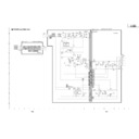
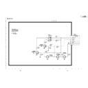
Monolithic Video Filter
* RH-iX3473CEZZ is 6.7MHz at Cut-off frequency.
* RH-iX3474CEZZ is 30MHz at Cut-off frequency.
* RH-iX3474CEZZ is 30MHz at Cut-off frequency.
»
Block Diagram
41
PZ-43MR2E
PZ-50MR2E
PZ-50MR2E
Ë
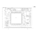
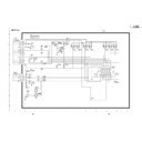
VHiFA3675F/-1 (ASSY: IC1702)
»
6-channel DC-DC Converter IC
»
Block Diagram
42
PZ-43MR2E
PZ-50MR2E
PZ-50MR2E
1
2
3
4
5
6
7
8
9
10
11
12
13
14
15
16
17
18
19
20
21
22
23
24
25
26
27
28
29
30
31
32
33
34
35
36
37
38
39
40
41
42
43
44
45
46
47
48
2
3
4
5
6
7
8
9
10
11
12
13
14
15
16
17
18
19
20
21
22
23
24
25
26
27
28
29
30
31
32
33
34
35
36
37
38
39
40
41
42
43
44
45
46
47
48
»
Pin Function
Pin No.
Pin Name
I/O
Pin Function
VCC1
RT
CT
CS3
CS5
CS4
CS1
CS2
VREF
CREF
VREG
IN2-
FB2
IN1-
FB1
IN5+
IN5-
FB5
IN6-
FB6
IN3+
IN3-
FB3
IN4+
IN4-
FB4
CP
GND
TLSEL
CNT5
CNT4
CNT2
CNT3
CNT1
VCC2
VDRV
PGND1
OUT1S
OUT1
OUT4
OUT3
OUT2S
OUT2
OUT6S
OUT6
OUT5
OUT5S
PGND2
RT
CT
CS3
CS5
CS4
CS1
CS2
VREF
CREF
VREG
IN2-
FB2
IN1-
FB1
IN5+
IN5-
FB5
IN6-
FB6
IN3+
IN3-
FB3
IN4+
IN4-
FB4
CP
GND
TLSEL
CNT5
CNT4
CNT2
CNT3
CNT1
VCC2
VDRV
PGND1
OUT1S
OUT1
OUT4
OUT3
OUT2S
OUT2
OUT6S
OUT6
OUT5
OUT5S
PGND2
—
—
—
—
—
—
—
—
—
—
—
—
—
—
—
O
O
O
O
O
I
O
I
O
I
I
I
O
I
O
I
I
I
O
I
I
I
O
I
—
I
I
I
I
I
I
I
I
I
I
I
—
O
—
O
O
O
O
O
O
O
O
O
O
O
O
O
O
O
O
O
O
O
—
Power supply for control circuit.
Oscillator timing resistor.
Oscillator timing capacitor.
Soft start for Ch.3 & Ch.4.
Soft start for Ch.6.
Soft start for Ch.5.
Soft start for Ch.1
Soft start for Ch.2.
Reference voltage output.
Capacitor for reference voltage output.
Regulated for voltage output.
Ch.2 inverting input to error amplifier.
Ch.2 output of error amplifier.
Ch.1 inverting input to error amplifier.
Ch.1 output of error amplifier.
Ch.5 non-inverting input to error amplifier.
Ch.5 inverting input to error amplifier.
Ch.5 output of error amplifier.
Ch.6 inverting input to error amplifier.
Ch.6 output of error amplifier.
Ch.3 non-inverting input to error amplifier.
Ch.3 inverting input to error amplifier.
Ch.3 output of error amplifier.
Ch.4 non-inverting input to error amplifier.
Ch.4 inverting input to error amplifier.
Ch.4 output of error amplifier.
Timing capacitor for timer latch delay.
Ground.
Ch.3 & Ch.4 timer latch selection(Low:disable).
Ch.6 ON/OFF function.
Ch.5 ON/OFF function.
Ch.2 ON/OFF function.
Ch.3 & Ch.4 ON/OFF function.
Ch.1 ON/OFF function.
Power supply for output stage.
Bias for logic circuit of output.
Power ground.
Ch.1 source electrode of output stage.
Ch.1 output(for Pch-MOSFET)
Ch.4 output(for Pch-MOSFET)
Ch.3 output(for Pch-MOSFET)
Ch.2 source electrode of output stage.
Ch.2 output(for Pch-MOSFET)
Ch.6 source electrode of output stage.
Ch.6 output(for Pch-MOSFET)
Ch.5 output(for Pch-MOSFET)
Ch.5 source electrode of output stage.
Power ground.
42
PZ-43MR2E
PZ-50MR2E
PZ-50MR2E
1
2
3
4
5
6
7
8
9
10
11
12
13
14
15
16
17
18
19
20
21
22
23
24
25
26
27
28
29
30
31
32
33
34
35
36
37
38
39
40
41
42
43
44
45
46
47
48
2
3
4
5
6
7
8
9
10
11
12
13
14
15
16
17
18
19
20
21
22
23
24
25
26
27
28
29
30
31
32
33
34
35
36
37
38
39
40
41
42
43
44
45
46
47
48
»
Pin Function
Pin No.
Pin Name
I/O
Pin Function
VCC1
RT
CT
CS3
CS5
CS4
CS1
CS2
VREF
CREF
VREG
IN2-
FB2
IN1-
FB1
IN5+
IN5-
FB5
IN6-
FB6
IN3+
IN3-
FB3
IN4+
IN4-
FB4
CP
GND
TLSEL
CNT5
CNT4
CNT2
CNT3
CNT1
VCC2
VDRV
PGND1
OUT1S
OUT1
OUT4
OUT3
OUT2S
OUT2
OUT6S
OUT6
OUT5
OUT5S
PGND2
RT
CT
CS3
CS5
CS4
CS1
CS2
VREF
CREF
VREG
IN2-
FB2
IN1-
FB1
IN5+
IN5-
FB5
IN6-
FB6
IN3+
IN3-
FB3
IN4+
IN4-
FB4
CP
GND
TLSEL
CNT5
CNT4
CNT2
CNT3
CNT1
VCC2
VDRV
PGND1
OUT1S
OUT1
OUT4
OUT3
OUT2S
OUT2
OUT6S
OUT6
OUT5
OUT5S
PGND2
—
—
—
—
—
—
—
—
—
—
—
—
—
—
—
O
O
O
O
O
I
O
I
O
I
I
I
O
I
O
I
I
I
O
I
I
I
O
I
—
I
I
I
I
I
I
I
I
I
I
I
—
O
—
O
O
O
O
O
O
O
O
O
O
O
O
O
O
O
O
O
O
O
—
Power supply for control circuit.
Oscillator timing resistor.
Oscillator timing capacitor.
Soft start for Ch.3 & Ch.4.
Soft start for Ch.6.
Soft start for Ch.5.
Soft start for Ch.1
Soft start for Ch.2.
Reference voltage output.
Capacitor for reference voltage output.
Regulated for voltage output.
Ch.2 inverting input to error amplifier.
Ch.2 output of error amplifier.
Ch.1 inverting input to error amplifier.
Ch.1 output of error amplifier.
Ch.5 non-inverting input to error amplifier.
Ch.5 inverting input to error amplifier.
Ch.5 output of error amplifier.
Ch.6 inverting input to error amplifier.
Ch.6 output of error amplifier.
Ch.3 non-inverting input to error amplifier.
Ch.3 inverting input to error amplifier.
Ch.3 output of error amplifier.
Ch.4 non-inverting input to error amplifier.
Ch.4 inverting input to error amplifier.
Ch.4 output of error amplifier.
Timing capacitor for timer latch delay.
Ground.
Ch.3 & Ch.4 timer latch selection(Low:disable).
Ch.6 ON/OFF function.
Ch.5 ON/OFF function.
Ch.2 ON/OFF function.
Ch.3 & Ch.4 ON/OFF function.
Ch.1 ON/OFF function.
Power supply for output stage.
Bias for logic circuit of output.
Power ground.
Ch.1 source electrode of output stage.
Ch.1 output(for Pch-MOSFET)
Ch.4 output(for Pch-MOSFET)
Ch.3 output(for Pch-MOSFET)
Ch.2 source electrode of output stage.
Ch.2 output(for Pch-MOSFET)
Ch.6 source electrode of output stage.
Ch.6 output(for Pch-MOSFET)
Ch.5 output(for Pch-MOSFET)
Ch.5 source electrode of output stage.
Power ground.
Oscillator timing resistor.
Oscillator timing capacitor.
Soft start for Ch.3 & Ch.4.
Soft start for Ch.6.
Soft start for Ch.5.
Soft start for Ch.1
Soft start for Ch.2.
Reference voltage output.
Capacitor for reference voltage output.
Regulated for voltage output.
Ch.2 inverting input to error amplifier.
Ch.2 output of error amplifier.
Ch.1 inverting input to error amplifier.
Ch.1 output of error amplifier.
Ch.5 non-inverting input to error amplifier.
Ch.5 inverting input to error amplifier.
Ch.5 output of error amplifier.
Ch.6 inverting input to error amplifier.
Ch.6 output of error amplifier.
Ch.3 non-inverting input to error amplifier.
Ch.3 inverting input to error amplifier.
Ch.3 output of error amplifier.
Ch.4 non-inverting input to error amplifier.
Ch.4 inverting input to error amplifier.
Ch.4 output of error amplifier.
Timing capacitor for timer latch delay.
Ground.
Ch.3 & Ch.4 timer latch selection(Low:disable).
Ch.6 ON/OFF function.
Ch.5 ON/OFF function.
Ch.2 ON/OFF function.
Ch.3 & Ch.4 ON/OFF function.
Ch.1 ON/OFF function.
Power supply for output stage.
Bias for logic circuit of output.
Power ground.
Ch.1 source electrode of output stage.
Ch.1 output(for Pch-MOSFET)
Ch.4 output(for Pch-MOSFET)
Ch.3 output(for Pch-MOSFET)
Ch.2 source electrode of output stage.
Ch.2 output(for Pch-MOSFET)
Ch.6 source electrode of output stage.
Ch.6 output(for Pch-MOSFET)
Ch.5 output(for Pch-MOSFET)
Ch.5 source electrode of output stage.
Power ground.

