Sharp LC-37P55E (serv.man12) Service Manual ▷ View online
44
LC-26GA5E
LC-32GA5E
LC-26P55E
LC-32P55E
LC-37P55E
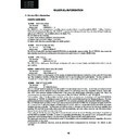
· IC1710:
Part number:
EPM3064
Sharp code:
RH-IXB716WJZZQ
This IC is a CPLD of Altera and use CMOS EEPROM cells to implement logic functions with 64 Macrocells. This
device controls ON/OFF power supply and signals for inverter unit.
FD604WJ (AV UNIT):
· IC301 & IC302 : AUDIO AMPLIFIER
Part number:
TDA8931T
Sharp code:
VHITDA893T-1Y
The TDA8931 is a switching power stage for high efficiency class-D audio power amplifier systems. The IC has a high
efficiency so that a heat sink is not required up to 20W (RMS).
· IC303 : HEADPHONE AMPLIFIER
Part number:
NJM4558M
Sharp code:
VHINJM4558M-1Y
The NJM4558 is a dual high-gain operational amplifier internally compensated and constructed on a single silicon
chip using an advanced epitaxial process.
· IC1101 & IC1102: VIDEO OUTPUT
Part number:
MM1506XN
Sharp code:
VHIMM1506XN-1Y
This IC extends the series of ICs for video/audio signal switching, with a 2-input 1-output single video switch with 75W
driver and input bias (6dB gain).
· IC1201: VIDEO INPUT
Part number:
MM1507XN
Sharp code:
VHIMM1506XN-1Y
This IC extends the series of ICs for video/audio signal switching, with a 2-input 1-output single video switch with
75W driver and input clamp.
FD605WJ (POWER SUPPLY UNIT):
· IC708:
Part number:
NJM2904M
Sharp code:
VHINJM2904M-1Y
The IC consists of two independent, high gain internally frequency compensated operation amplifiers which were
designed specifically to operate from single power supply.
· IC706 & IC707: FEEDBACK CONTROL
Part number:
TA76431R
Sharp code:
VHITA76431R-1Y
Adjustable precision shunt regulator for feedback control for driving an optocoupler in power supplies
· IC705: POWER SUPPLY CONTROLLER FOR INVERTER
Part number:
MR4020
Sharp code:
VHIMR4020++-1
A high speed 900V IGBT makes ideal partial resonance operation which ensures high efficiency and low noise.
Very low power consumption at micro-loads (burst mode).
Start-up circuit eliminates the need for start-up resistor.
Excess current protection (ON period limitation, primary current limitation), excess voltage protection, and thermal
shut-down function are incorporated.
·
IC704: POWER SUPPLY CONTROLLER FOR SIGNAL BOARD
Part number:
MR4020
Sharp code:
VHIMR4020++-1
A high speed 900V IGBT makes ideal partial resonance operation which ensures high efficiency and low noise.
45
LC-26GA5E
LC-32GA5E
LC-26P55E
LC-32P55E
LC-37P55E
Very low power consumption at micro-loads (burst mode).
Start-up circuit eliminates the need for start-up resistor.
Excess current protection (ON period limitation, primary current limitation), excess voltage protection, and thermal
shut-down function are incorporated.
FD607WJ (RC/LED UNIT):
·
IC101 : OPC
Part number:
TPS850
Sharp code:
VHITPS850++-1Y
The TPS850 is a linear-output photo-IC which incorporates a photodiode and current amp circuit in a single chip. This
photo-IC is current output type, so can set up output voltage freely by arbitrary load resistance.
FD608WJ (TUNER UNIT):
· IC201 : IF-Demodulator/PLL
Part number:
TDA9886
Sharp code:
VHITDA9886+-1Y
The TDA9886 is an alignment-free multi-standard (PAL, SECAM and NTSC) vision and sound IF signal PLL
demodulator for positive and negative modulation including sound AM and FM processing.
This IC features the following.
* Gain controlled wide-band vision intermediate frequency (VIF) amplifier (AC-coupled).
* Multi-standard true synchronous demodulation with active carrier regeneration (very linear demodulation,
good intermodulation figures reduced harmonics, excellent pulse response).
* Gate phase detector for L/L accent standard.
* Fully integrated VIF Voltage Controlled Oscillator (VCO), alignment-free; frequencies switchable for all
negative modulated standards via I2C bus.
* 4MHz reference frequency input [signal from phase-locked loop (PLL) tuning system] or operating as crystal
oscillator.
* VIF Automatic Gain Control (AGC) detector for gain control operating as a peak sync detector for negative
modulated signals and as a peak white detector for positive modulated signals.
46
LC-26GA5E
LC-32GA5E
LC-26P55E
LC-32P55E
LC-37P55E
2. Detailed ICs Information
SiI 9021
SiI-DS-0117
Pin Diagram
144-Pin
TQFP
SiI 9021
(Top View)
Figure 1. Pin Diagram
2.1. IC1905 (VHISII9021+-1Q)
2.1.1. Pinning
2.1.2. Block Diagram
SiI 9021
SiI-DS-0117
SiliconImage Confidential
For
Sharp
Internal use Only
Functional Description
SiI 9021
SiI 9021
PanelLink
TMDS
PanelLink
TMDS
Figure 3. Functional Block Diagram
SiI 9021
The SiI 9021 supports two HDMI input ports. Only one port may be active at any time.
47
LC-26GA5E
LC-32GA5E
LC-26P55E
LC-32P55E
LC-37P55E
2.2. IC3002 (RH-IXB624WJZZQ)
2.2.1. Pin Connections and Short Description
ADVANCE INFORMATION
VCT 69xyP
Volume 1: General Description
Micronas
November 3, 2004; 6251-644-1-1
AI
1-55
3.12.Pin Connections and Short Description
NC = not connected
LV = if not used, leave vacant
OBL = obligatory; connect as described in circuit
diagram
IN = Input Pin
ANA = Analog Pin
OUT = Output Pin
SUPPLY = Supply Pin
VCTP Pin No.
Pin Name
Type
Connection
Short Description
PLQFP
208-1
(If not used)
1
656O6
P4_6
TDOFW
IN/OUT
LV
Digital 656 Bit 6 Output
Port 4, Bit 6 Input/Output
JTAG Interface Data Output (firmw. Controler)
2
656O5
P4_5
TDIFW
IN/OUT
LV
Digital 656 Bit 5 Output
Port 4, Bit 5 Input/Output
JTAG Interface Data Input (firmw. Controler)
3
656O4
P4_4
TMSFW
IN/OUT
LV
Digital 656 Bit 4 Output
Port 4, Bit 4 Input/Output
JTAG Interface Mode Select Input (fw. Contr.)
4
656O3
P4_3
TCLK
IN/OUT
LV
Digital 656 Bit 3 Output
Port 4, Bit 3 Input/Output
JTAG Interface Clock Input (TV Controler)
5
656O2
P4_2
TDO
IN/OUT
LV
Digital 656 Bit 2 Output
Port 4, Bit 2 Input/Output
JTAG Interface Data Output (TV Controler)
6
656O1
P4_1
TDI
IN/OUT
LV
Digital 656 Bit 1 Output
Port 4, Bit 1 Input/Output
JTAG Interface Data Input (TV Controler)
7
656O0
P4_0
TMS
IN/OUT
LV
Digital 656 Bit 0 Output (LSB)
Port 4, Bit 0 Input/Output
JTAG Interface Mode Select Input (TV Contr.)
8
RESETQ
IN/OUT
OBL
Reset Input/Output
9
AIN1R
IN
GND
Analog Audio 1 Input, Right
10
AIN1L
IN
GND
Analog Audio 1 Input, Left
11
AIN2R
IN
GND
Analog Audio 2 Input, Right
12
AIN2L
IN
GND
Analog Audio 2 Input, Left
13
AIN3R
IN
GND
Analog Audio 3 Input, Right
14
AIN3L
IN
GND
Analog Audio 3 Input, Left
15
AIN4R
IN
GND
Analog Audio 4 Input, Right
16
AIN4L
IN
GND
Analog Audio 4 Input, Left
17
VREFAU
ANA
OBL
Reference Voltage, Audio
18
VSUP8.0AU
SUPPLY
OBL
Supply Voltage Analog Audio, 8.0 V
19
GNDA
SUPPLY
OBL
Ground Analog Audio, Platform Ground
20
SGND
ANA
OBL
Analog Signal GND

