Sharp LC-37AD1E (serv.man10) Service Manual ▷ View online
55
55-1
55-2
LC-37AD1E
Ë
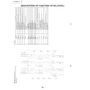
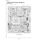
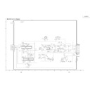
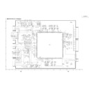
VHITB1274AF1EQ (ASSY:IC801)
VIDEO/CHROMA/SYNC. processor
»
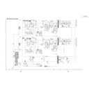
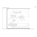
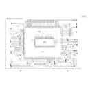
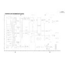
Block Diagram
»
Pin Function
Pin No
.
P
in Name
I/O
Pin Function
1
CVBS1/Y1-IN
I
CVBS1 or a Y1-IN signal is inputted.
2
SYNC-IN
I
Synchronized signal is inputted.
3
CVBS-OUT
O
O
utput terminal of CVBS or a Y+C signal.
4
V
S
O
Counted-down vertical synchronized signal is outputted.
5
COMB Y-IN
I
Y
-signal outputted from comb-filter is inputted.
It opens, when not using it.
6
D-VDD
—
Power supply of a DDS/BUS/V-CD/H-CD block is supplied.
DC5V (standard)"
7
COMB C-IN
I
C-signal outputted from comb-filter is inputted.
It opens, when not using it."
8
D
-GND
—
GND terminal of a DDS/BUS/V-CD/H-CD block.
9
H
S
O
Horizontal synchronized signal which required H-AFC is outputted.
10
SCP
O
Sand Castle Pulse is outputted. A clamp pulse and a horizontal Blanking pulse
are outputted.
11
Yvi-IN
O
Y
-signal for a synchronous input selected by Video-SW is outputted.
12
SYNC-VCC
—
Power supply of a SYNC/HVCO block is supplied.
DC5V (standard)
13
SCL
I
SCL terminal of I2CBUS.
14
SDA
I/O
SDA terminal of I2CBUS.
15
YS3(RGB1-in)
I
S
electe SW of a main signal and RGB1 input signal.
Only when "RGB1-ENB" is set as "enable" by bus setup, the input of YS3
becomes effective.
16
SYNC-GND
—
GND terminal of a SYNC/HVCO block.
17
Cr1-IN
I
Y1-/Cb1/Cr1 signal is inputted.
18
Cb1-IN
I
19
Y1-IN
I
20
CLP-FIL
—
Filter for Y clamp is connected.
21
Y-OUT
O
Y/Cb/Cr signal is outputted.
22
Cb-OUT
O
23
Cr-OUT
O
24
YS1(YVbC2-IN)
I
Selecte SW of a main signal and YCrCb2 input signal.
25
B1-IN
I
RGB1 signal is inputted. This input is selected in YS3 or I2CBUS.
26
G1-IN
I
27
R1-IN
I
28
Y/C-GND
—
GND terminal of Y/C/Text/Video-SW / 1HDL block.
29
Cr2-IN
I
Y2/Cb2/Cr2 signal is inputted. This input is selected in YS1.
It opens, when not using it.
30
Cb2-IN
I
31
Y2-IN
I
32
Y/C-VCC
—
Power supply of Y/C/Text/Video-SW / 1HDL block is supplied.
DC5V (standard)
33
B2-IN
I
RGB2 signal is inputted. This input is selected in YS2.
It opens, when not using it.
34
G2-IN
I
35
R2-IN
I
36
YS2/YM(RGB2-IN)
I
S
electe SW of a main signal and RGB2 input signal.
37
FIL.
—
Connects with a Y/C-VCC terminal.
38
X'TAL
—
16.2MHz X'tal oscillation element is connected.
39
C3-IN
I
Chrominance signal is inputted. It opens, when not using it.
40
APC-FIL
—
Filter for a chrominance demodulater is connected.
41
CVBS3/Y3-IN
I
CVBS3 or Y3 signal is inputted. It opens, when not using it.
42
ADDRESS
I
S
lave address is set up.
43
C2-IN
I
Chrominance signal is inputted. It opens, when not using it.
44
CVBS2/Y2-IN
I
CVBS2 or Y2 signal is inputted. It opens, when not using it.
45
COMB SYS
O
The distinction result of the received color system is outputted from this terminal
and a terminal 46.
46
Fsc-OUT
O
Subcarrier is outputted.
47
AFC-FIL
—
Filter for AFC detection is connected.
48
C1-IN
I
Chrominance signal is inputted. It opens, when not using it.
56
56-1
56-2
LC-37AD1E
»
Pin Function
Pin No
.
P
in Name
I/O
Pin Function
1
IN2-H
I
IN2-H:FIndependent H-synchronization signal input terminal
2
IN2-V
I
IN2-V:FIndependent V-synchronization signal input terminal
3
IN2-1
I
Signal input terminal of IN2 system
4
IN2-2
I
5
IN2-3
I
6
V
cc-MAT
—
Power supply terminal of a selector system and a synchronous processing
system
7
IN3-H
I
IN3-H:FIndependent H-synchronization signal input terminal
8
IN3-V
I
IN3-V:FIndependent V-synchronization signal input terminal
9
IN3-1
I
Signal input terminal of IN3 system
10
IN3-2
I
11
IN3-3
I
12
GND-MAT
—
Ground terminal of a selector system and a synchronous processing system
13
IN4-H
I
IN4-H:FIndependent H-synchronization signal input terminal
14
IN4-V
I
IN4-V:FIndependent V-synchronization signal input terminal
15
IN4-1
I
Signal input terminal of IN4 system
16
IN4-2
I
17
IN4-3
I
18
V-PH
—
Capacitor connection terminal for carrying out the peak hold of the V-sync.
19
IN5-H
I
IN5-H
Å
FIndependent H-synchronization signal input terminal
20
IN5-V
I
IN5-V
Å
FIndependent V-synchronization signal input terminal
21
IN5-1
I
Signal input terminal of IN5 system
22
IN5-2
I
23
IN5-3
I
24
H-PH
—
Capacitor connection terminal for carrying out the peak hold of the H-sync.
25
YG-OUT
O
Composite Video signal output terminal for synchronous separation.
26
YG-IN
I
Composite Video signal input terminal for synchronous separation.
27
IREF-SYNC
—
Reference current setting terminal (about 4.6 V)
28
VS-OUT
O
HV of IN1 system or HV of IN2 to IN5 system selector output, and this either are
chosen by I2 C BUS"YCBCR/MAT", and it outputs by positive.
29
HS-OUT
O
30
Vcc-OUT
O
P
ower supply terminal of RGB system
31
SCP-IN
I
Input terminal of Sand-Castle-Pulse
32
VTIM-IN
I
Input terminal of V-timing pulse.
33
HP-IN
I
Input terminal of H-pulse
34
GND-OUT
O
G
round terminal of RGB system
35
R-OUT
O
O
utput terminal of RGB signal
37
G-OUT
O
Outputted by 2.6 Vp-p at the time of the input of the white of 100IRE.
39
B-OUT
O
36
R-SH
—
Sample & Hold terminal for AKB of RGB
38
G-SH
—
40
B-SH
—
41
IK-IN
I
Reference pulse is returned to this terminal.
42
PABL-FIL
I
Peak hold terminal of Peak ABL.
43
ABL-FIL
I
LPF is formed to an ABL control signal.
44
ABL-IN
I
ABL control signal input terminal
45
YS/YM-1
I
Control input terminal of YM1/YS1
Input level corresponds with three values.
When the value of YM and each YS reaches, it serves also as the function
which turns off VM.
46
LR1-IN
I
S
ignal input terminal of analog RGB1
47
LG1-IN
I
48
LB1-IN
I
49
YS/YM-2
I
Control input terminal of YM2/YS2
Input level corresponds with three values.
When the value of YM and each YS reaches, it serves also as the function
which turns off VM.
50
LR2-IN
I
S
ignal input terminal of analog RGB2
51
LG2-IN
I
52
LB2-IN
I
53
ADDRESS
I
S
lave address setting terminal of I2C BUS.
54
DPIC-C
—
Capacitor is connected to black detection of dynamic picture (black extension)
at GND.
55
SCL
I
Input terminal of SCL(Serial Clock) of a I2C BUS standard.
56
SDA
I
Input terminal of SDA(Serial Data) of a I2C BUS standard.
57
DPIC-MUTE
I
MUTE of dynamic picture (black extension) is controllable with a terminal.
58
CLP-C
C
onnection terminal of the capacitor for Y-system clamp.
Ë
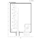
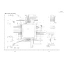
VHICXA2101Q-1Q(ASSY:IC803)
Multi Component Processor
»
Block Diagram
57
57-1
57-2
LC-37AD1E
Pin No
.
Pin Name
I/O
Pin Function
59
VM-OUT
O
VM output terminal. The differentiation waveform of Y-signal is outputted by
positive.
60
VM/SHP/
—
Terminal for turning off VM, SHARPNESS, and COLOUR.
COL-OFF
Input level corresponds with three values.
61
YCBCR-SW
I
Change terminal of a signal inputted into INT/EXT SW.
External input terminal is chosen by High.
62
ECR-IN
I
Input terminal of Exteriors Y, Cb and Cr.
63
ECB-IN
I
64
EY-IN
I
65
V1-IN
I
Input terminal of HV of IN1 system. Positive input.
66
H1-IN
I
67
CR1-IN
I
Input terminal of Y, Cb, and Cr of IN1 system.
68
CB1-IN
I
69
Y1-IN
I
70
GND-SIG
—
GND terminal of the signal processing system of Y-component
71
IREF-YC
—
Reference current setting terminal (mainly Y-component signal processing
system).
72
Vcc-SIG
—
Power supply terminal of the signal processing system of Y-component.
73
SELCR-IN
I
Selector outputs Y, Cb, and Cr are inputted through the capacitor for a clamp.
74
SELCB-IN
I
75
SELY-IN
I
76
SELY-OUT
O
Selector output terminal of IN2 to IN5.
The signal changed into Y, Cb, and Cr is outputted.
77
SELCB-OUT
O
78
SELCR-OUT
O
79
SELH-OUT
O
Selector HV output terminal of IN2 to IN5.
80
SELV-OUT
O
Ë
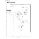
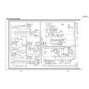
VHIMM1519XQ-1Q(IC1401)
Component input video switch
»
Block Diagram
Pin No
.
P
in Name
I/O
Pin Function
»
Pin Function
1
V
IDEO 1-L1
I
L
ine input of D-terminal
2
V
IDEO 1-L2
I
3
V
IDEO 1-L3
I
11
VIDEO 2-L1
I
12
VIDEO 2-L2
I
13
VIDEO 2-L3
I
21
VIDEO 3-L1
I
22
VIDEO 3-L2
I
23
VIDEO 3-L3
I
4,14,39,45,52,58
VCC
—
Analog power supply(9V)
51
AVCC
—
5
VIDEO 2-Y
I
Y-signal input
15
VIDEO 3-Y
I
53
TUNER-Y
I
59
VIDEO 1-Y
I
24
DGND
—
GND
6,8,16,18,33,35,
GND
—
37,41,43,47,49,
54,56,60,62
7
V
IDEO 2-Pb
I
Pb,Pr signal input
9
V
IDEO 2-Pr
I
17
VIDEO 3-Pb
I
19
VIDEO 3-Pr
I
55
TUNER-Pb
I
57
TUNER-Pr
I
61
VIDEO 1-Pb
I
63
VIDEO 1-Pr
I
10
VIDEO 2-SW
I
Switch line of D-terminal
20
VIDEO 3-SW
I
32
MONO-SW
I
64
VIDEO 1-SW
I
25
ADDRESS
I
S
lave address select pin
26
SDA
I/O
Data input of I2C bus
27
SCL
I
Clock input of I2C bus
28
DVCC
—
Digital power supply(5V)
29
L3 OUT
O
Line output for monitor
30
L2 OUT
O
31
L1 OUT
O
34
Pr OUT 3
O
Video signal output
36
Pb OUT 3
O
38
Y OUT 3
O
40
Pr OUT 2
O
42
Pb OUT 2
O
44
Y OUT 2
O
46
Pr OUT 1
O
48
Pb OUT 1
O
50
Y OUT 1
O
58
58-1
58-2
LC-37AD1E
Ë
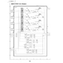
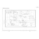
VHICXA2069Q-1 (ASSY:IC1301)
S2 correspondence 7 input 3 output AV switch
»
Block Diagram
»
Pin Function
Pin No
.
Pin Name
I/O
Pin Function
63
TV
I
Video signal input
1
V
1
I
Composite video signal input
8V
2
I
15
V3
I
22
V4
I
30
V5
I
60
V6
I
3
Y
1
I
Luminance signal is inputted with a Y/C separation signal input terminal.
10
Y2
I
YIN1 inputs the signal which carried out Y/C separation of the output of VOUT1.
17
Y3
I
24
Y4
I
49
YIN1
I
5
C
1
I
Chrominance signal is inputted with the input terminal of Y/C separation signal.
12
C2
I
CIN1 inputs the signal which carried out Y/C separation of the output of VOUT1.
19
C3
I
26
C4
I
51
CIN1
I
62,2
LTV,LV1
I
Input terminal of an audio signal
9,16
LV2,LV3
I
23,29
LV4,LV5
I
59,64
LV6,RTV
I
4,11
RV1,RV2
I
18,25
RV3,RV4
I
31,61
RV5,RV6
I
53
VOUT1
O
Composite video signal is outputted with the output terminal of a video signal.
41
VOUT3
O
44
V/YOUT2
O
Composite video signal output or a luminance signal output is chosen with the
output terminal of a video signal in I2C Bus control.
56
YOUT1
O
Luminance signal is outputted with the output terminal of a video signal.
39
YOUT3
O
58
COUT1
O
Chrominance signal is inputted with the output terminal of a video signal.
47
COUT2
O
37
COUT3
O
52
LOUT1
O
Audio signal output terminal
43
LOUT2
O
38
LOUT3
O
54
ROUT1
O
45
ROUT2
O
40
ROUT3
O
6
S2-1
I
Terminal on which C-signal was overlapped and which detects DC of S2
13
S2-2
I
correspondence.
20
S2-3
I
Less than 1.3V and they are 4:3 picture signals.
27
S2-4
I
More than 1.3V and less than 2.5V, and is a 4:3 letter box signal.
More than 2.5V and is the squeeze signal of 16:9 pictures.
GND at 100K
Ω
pull-down Since it is carrying out, it becomes 4:3 picture signals
at the time of opening.
7
S-1
I
Terminal for a change of composite video/S.
14
S-2
I
D
etection result is written in a status register.
21
S-3
I
Less than 3.5V and is S-signal. More than 3.5V and is a composite video signal.
28
S-4
I
Since the pull-up is carried out to 5V by resistance of 100K
É
, it becomes a
composite video signal at the open.
32
ADR
I
I2C Choose the slave address for Bus.
Less than 1.5V and is 90H. More than 2.5V and is 92H. Set to 90H at the time
of terminal opening.
33
SCL
I
Signal input terminal for I2C Bus.
34
SDA
I
Signal input terminal for I2C Bus.
36
DC OUT
O
D
C of the S2 correspondence superimposed on COUT3 output is outputted.
DC is superimposed by connecting with COUT3 output through capacity. Control
by I
2
CBus.
When external resistance 4.7Kohm is attached, output impedance 10±3K
Ω
of
S2 standard is realized.
55
TRAP1
I
Trap circuit for subcarriers is connected.
46
TRAP2
I
48
MUTE
I
Mute terminal for audio signal output
Less than 1.3V and is the mute off.
More than 2.5V and is the mute on.
50
BIAS
I
Terminal for internal reference bias (Vcc/2).
Connects with GND through a capacitor.

