Sharp LC-37AD1E (serv.man10) Service Manual ▷ View online
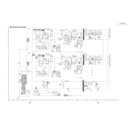
69
69-1
69-2
LC-37AD1E
»
Pin Function
36, 37, 38,
D23-D12
I
Upper 12 bits of 24-bit pixel bus. Mode controlled by configuration register bit:
39, 40, 41,
When BSEL = HIGH, this bus inputs the top half of the 24-bit pixel bus.
42, 43, 44,
When BSEL = LOW, these bits are not used to input pixel data. In this mode,
45, 46, 47
the state of D[23:16] is input to the I2C register CFG. This allows an extra 8-bits
of user configuration data to be read by the graphics controller through the I2C
interface (see I2C register definition).
50, 51, 52,
D11-D0
I
Bottom half of 24-bit pixel bus / 12-bit pixel bus input. Mode controlled by
53, 54, 55,
configuration register bit:
58, 59, 60,
When BSEL = HIGH, this bus inputs the bottom half of the 24-bit pixel bus.
61, 62, 63
When BSEL = LOW, this bus inputs _ a pixel (12-bits) at every latch edge (both
falling and/or rising) of the clock.
Ë
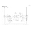
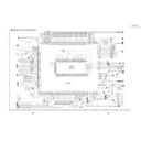
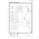
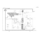
9DK001-15106(ASSY:IC10413)
SiI170 Panel Link Transmitter
»
Block Diagram
Pin No
.
Pin Name
I/O
Pin Function
Pin No
.
P
in Name
I/O
Pin Function
57
IDCK+
I
Input Data Clock +. This clock is used for all input modes.
56
IDCK-
I
Input Data Clock -. This clock is only used in 12-bit mode when dual edge
clocking is turned off (DSEL = LOW). It is used to provide the ODD latching
edges for multi-phased clocking. If (BSEL = HIGH) or (DSEL = HIGH) this pin is
unused and should be tied to GND.
2
D
E
I
Data enable. This signal is high when input pixel data is valid to the transmitter
4
H
SYNC
I
Horizontal Sync input control signal.
5
V
SYNC
I
Vertical Sync input control signal.
3
VREF
I
Must be tied to 3.3V.
10
PD#
I
Power Down (active LOW). A HIGH level (3.3V) indicates normal operation and
a LOW level (GND) indicates power down mode. During power down mode, the
I2C pins are active, but digital input, output buffers and the PanelLink Digital
core are powered down. This pin should be tied LOW to ensure the chip is
powered off when RESET is asserted.
When PD# is asserted, the differential output pins for TMDS are tri-stated until
the PD# register bit is asserted through I2C.
25
TX0+
TMDS Low Voltage Differential Signal output data pairs.
24
TX0-
These pins are tri-stated when PD# is asserted.
28
TX1+
27
TX1-
31
TX2+
30
TX2-
22
TXC+
TMDS Low Voltage Differential Signal output clock pairs.
21
TXC-
These pins are tri-stated when PD# is asserted.
19
EXT_SWING
Voltage Swing Adjust. A resistor should tie this pin to AVCC. This resistor
determines the amplitude of the voltage swing. A 510 ohm resistor is
recommended for remote display applications. For notebook computers, 680
ohm is recommended.
11
MSEN
O
Monitor Sense. This pin is an open collector output. The output is
programmable through the I2C interface (see I2C register definitions). An
external 5K pull-up resistor is required on this pin.
34
I
normal operation.
7, 8
N
C
—
These pins are not electrically connected inside the package.
13
ISEL/RST#
I
I2C Interface Select. If HIGH, then the I2C interface is active.
15
SCLS
I
DDC I2C Clock. This pin is a slave I2C clock line which interfaces to the DDC
bus for communicating with a host side master. HDCP KSV, An, and Ri values
are exchanged over this DDC bus during authentication. The clock may be run
up to 400kHz. This pin is not 5V-tolerant; it should be connected through a level
shifter to the DDC clock line SCL. This is an open-collector pin.
14
SDAS
I/O
DDC I2C Data. This pin is a slave I2C data line for communicating with a host
side master. HDCP KSV, An, and Ri values are exchanged over this DDC bus
during authentication. Data may be clocked in at up to 400kHz. This pin is not
5V-tolerant; it should be connected through a level shifter to the DDC clock line
SDA. This is an open-collector bi-directional pin, and is not made high-
impedance when PD#=LOW.
6
CTL3
I
External CTL3. This pin is used to bring in the CTL3 signal for HDCP when the
HDCP encryption is performed before the video enters the SiI 170. To enable
this input, the CTL3 bit must be programmed in Reg[0x08]. If the CTL3 bit is
cleared, then this input pin is ignored and may be left unconnected. This pin is a
regular high swing (3.3V) input, containing a weak pull-down resistor so that if
left unconnected it will default to LOW.
9
H
TPLG
I
Monitor Charge Input. This pin is used to connect to the DVI Hot Plug pin to
detect the presence of an attached monitor.
1,12,33
VCC
—
Digital VCC. Connect to 3.3V supply.
16,35,64
GND
—
Digital GND.
23,29
AVCC
—
Analog VCC. Connect to 3.3V supply.
20,26,32
AGND
—
Analog GND.
18
PVCC1
—
Primary PLL Analog VCC. Connect to regulated 3.3V supply.
49
PVCC2
—
Filter PLL Analog VCC. Connect to regulated 3.3V supply.
17
PGND1
—
PLL Analog GND.
48
PGND2
—
PLL Analog GND.

