Sharp LC-30HV4E (serv.man9) Service Manual ▷ View online
33
LC-30HV4E
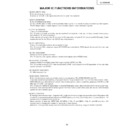
MAJOR IC FUNCTIONS INFORMATIONS
∫
IC2501 (MSP4418G)
IC for decoding audio signals.
It serves as an S-IF audio signal decoder and an audio data selector.
IC for decoding audio signals.
It serves as an S-IF audio signal decoder and an audio data selector.
∫
IC2510 (IXA385WJ)
IC for controlling audio delay.
LC-30/37HV4E uses a frame buffer to process video signals. This results in delay in outputting video signals.
The IC delays output of audio signals to synchronize output of video and audio signals.
IC for controlling audio delay.
LC-30/37HV4E uses a frame buffer to process video signals. This results in delay in outputting video signals.
The IC delays output of audio signals to synchronize output of video and audio signals.
∫
IC1301 (CXA2069Q)
7-input, 3-output selector.
This IC selects all audio and video signals received from input terminals and the tuner, except those signals
that relates to PC and components.
Video signals delivered to the IC are sent to YC separation circuits IC401 (main) and IC402 (sub). Audio
signals are sent to the SR unit via IC2501 (sound processor).
∫
IC401 (MM1519XQ)
4-input, 3-output video selector for component input.
This IC receives AV3 component input, AV1/3 RGB input and teletext RGB signals. Its output is for main, sub
and component.
4-input, 3-output video selector for component input.
This IC receives AV3 component input, AV1/3 RGB input and teletext RGB signals. Its output is for main, sub
and component.
∫
IC1601 (SDA5550M)
Teletext processing microcomputer.
This IC receives vide signals, decodes teletext and outputs data in RGB format.
Teletext processing microcomputer.
This IC receives vide signals, decodes teletext and outputs data in RGB format.
∫
IC401/IC402 (TC90A69)
Adaptive infield 3-line digital comb filter supporting both NTSC and PAL.
This IC is a high-precision Y/C 1 chip incorporating a CNR circuit and performs YC separation of the sub video
signals received from IC1301.
Adaptive infield 3-line digital comb filter supporting both NTSC and PAL.
This IC is a high-precision Y/C 1 chip incorporating a CNR circuit and performs YC separation of the sub video
signals received from IC1301.
∫
IC403/IC404 (ML6428C1)
6.7 MHz low-pass filter.
6.7 MHz low-pass filter.
∫
IC801/IC802 (TB1274AF)
IC for synchronous processing of video and chroma signals for PAL/NTSC/SECAM color TV.
Color demodulation is provided by a high-performance image compensation circuit in the video section, a PAL/
NTSC/SECAM auto discrimination circuit in the chroma section, and a crystal that generates 4.43 MHz, 3.58
MHz and M/N-PAL clock signals.
This IC has a 4-channel YC signal input, 2-channel RGB signal input, and 2-channel chrominance signal input.
It receives main and sub chrominance signals from IC401 (main) and IC402 (sub) and delivers chrominance
signals via one-channel output.
∫
IC803 (CXA2101Q)
IC having a chrominance input integrated with a high-performance image compensation circuit. Equipped with
circuits for processing baseband signals and RGB signals and a 4-channel video switch incorporating an H/V
synchronization signal processing circuit.
Input selection is done by INPUT-SEL (IIC BUS). Y, Pb, Pr and GBR of Ycb, Cr and HD and their H/V
synchronization signals are inputted to input pins of each channel.
Multi-scan facility permits acceptance of a horizontal scan line frequency range of 16 KHz to 60 KHz.
34
LC-30HV4E
∫
IC1901 (IXA392WJ)
FPGA for synchronous processing
This IC selects synchronization signals and creates horizontal blanking signals.
FPGA for synchronous processing
This IC selects synchronization signals and creates horizontal blanking signals.
∫
IC604 (TA1318AF)
IC for synchronous processing of TV component signals and measurement of frequency.
This IC incorporates an input signal frequency measurement feature and synchronous regeneration features.
It supports synchronous horizontal regeneration (15.75 KHz, 31.5 KHZ, 33.75 KHz and 45 KHz) and synchronous
vertical regeneration (525I, 525P, 625I and 750P).
PC I/F board side
∫
IC4 (CX3506R)
3-channel, 8-bit, 120 MSPS A/D converter incorporating AMP and PLL.
This IC is for video signals inputted to the IF board and used for one-screen and two-screen applications, and
for PC signals inputted to the front panel.
It provides A/D conversion of video signals (analog RGB) inputted to IN1 from CN6 and PC signals (analog
RGB) inputted to IN2 from CN8.
Converted digital signals are sent to IC25.
∫
IC310 (TLC5733A)
3-channel, 8-bit, 20 MSPS A/D converter.
This IC is for video signals inputted to the IF board and used for two-screen application.
It provides A/D conversion of video signals (analog YcbCr) inputted to IC310 from CN6.
Converted digital signals are sent to IC25.
3-channel, 8-bit, 20 MSPS A/D converter.
This IC is for video signals inputted to the IF board and used for two-screen application.
It provides A/D conversion of video signals (analog YcbCr) inputted to IC310 from CN6.
Converted digital signals are sent to IC25.
∫
IC25 (IXA091WJ)
IC for I/P conversion and scaling of digital image according to the output resolution, and for data conversion.
There are two input channel: V0 and V1. V1 is for sub 480i/580i input processing for two-screen application. V0
is for processing all signals for main used for one and two-screen applications.
The IC generates clamp signals based on input synchronization signals.
It also performs data matrix conversion, and creates OSD signals.
Processed signals are sent to IC413.
∫
IC413 (SiI170)
Panel link transmitter.
This IC converts 8-bit RGB image data received from IC25 into TMDS differential signals and sends to the
monitor.
Panel link transmitter.
This IC converts 8-bit RGB image data received from IC25 into TMDS differential signals and sends to the
monitor.
∫
IC1 (IX8270CE)
One-chip RISC microprocessor.
This IC communicates with the monitor and controls the system operation.
It controls all the ICs located in the media receiver.
One-chip RISC microprocessor.
This IC communicates with the monitor and controls the system operation.
It controls all the ICs located in the media receiver.
∫
IC405 (UPD4721G)
RS-232 line driver/receiver conforming to EIA/TIA-232-E.
This IC enables the system to be controlled from a PC connected to the system.
It also allows IC1 to be upgraded using the PC.
RS-232 line driver/receiver conforming to EIA/TIA-232-E.
This IC enables the system to be controlled from a PC connected to the system.
It also allows IC1 to be upgraded using the PC.
35
LC-30HV4E
Pin No.
Pin Name
Type
Description
1, 19, 32, 33
VDD
––
Power supply
44, 64
2
PLLVDC
––
PLL power supply
3
VCOIN
I
VCO IN (used to construct external loop filter)
4
TEST
I
Input for testing
5
CPOUT
O
Charge pump out (used to construct external loop filter)
6
PLLEN
I
PLL enable signal input
7
PLLGND
––
8, 9, 10, 18, 31
GND
––
41, 42, 43, 62
11
PLLENO
O
PLL enable signal output
12
SPDIFO
O
S/PDIF output (3.072 Mbps)
13
SPDIFI
I
S/PDIF input (3.072 Mbps)
14
IO0
I/O
Expanded I/O, bit 0
15
IO1
I/O
Expanded I/O, bit 1
16
IO2
I/O
Expanded I/O, bit 2
17
IO3
I/O
Expanded I/O, bit 3
20
IO4
I/O
Expanded I/O, bit 4
21
UTEST
I
Input for testing
22
NANDTO
O
Output for testing
23
RESET
I
Asynchronous reset signal input
24
MEMTEST
I
Input for testing
25
BISTOUT
O
Output for testing
26
RWCLK
O
Expanded FIFO R/W clock
27
RSTRW
O
Expanded FIFO master reset
28
FEW
O
Expanded FIFO write enable
29
FRE
O
Expanded FIFO read enable
30
FD07
O
Expanded FIFO data output, bit 7
34
FD06
O
Expanded FIFO data output, bit 6
35
FD05
O
Expanded FIFO data output, bit 5
36
FD04
O
Expanded FIFO data output, bit 4
37
FD03
O
Expanded FIFO data output, bit 3
38
FD02
O
Expanded FIFO data output, bit 2
39
FD01
O
Expanded FIFO data output, bit 1
40
FD00
O
Expanded FIFO data output, bit 0
45
FD17
I
Expanded FIFO data input, bit 7
46
FD16
I
Expanded FIFO data input, bit 6
47
FD15
I
Expanded FIFO data input, bit 5
48
FD14
I
Expanded FIFO data input, bit 4
49
FD13
I
Expanded FIFO data input, bit 3
50
FD12
I
Expanded FIFO data input, bit 2
51
FD11
I
Expanded FIFO data input, bit 1
52
FD10
I
Expanded FIFO data input, bit 0
53
SDA
I/O
Serial communication data
54
SCS
I
Serial communication chip select
55
SCK
I
Serial communication chip select
56
I2SCLO
O
12S CL output
57
I2SDAO
O
12S CL output
58
I2SWSO
O
12S WS output
59
I2SWSI
I
12S WS input
60
I2SDAI
I
12S DA input
61
I2SCLI
I
12S CL input
63
REFCLK
I
PLL REF CLK (same input as 12SCLI)
Ë
RH-iXA385WJZZ (ASSY:IC2510)
»
Pin mapping
36
LC-30HV4E

