Sharp LC-19D1EWH (serv.man6) Service Manual ▷ View online
LC-19D1E/S-BK/WH
5 – 4
2. Detailed ICs Information
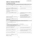
2.1. IC202 (RH-iXB964WJZZQ) (STV0362)
2.1.1 Block Diagram
2.1.2 Pin Connections and short description
DVB-T RECEIVER
Pin No
Pin Name
I/O
Pin Function
32
NOT_RESET
I
Hardware reset, active Low.
15
XTAL_I
I
Crystal oscillator input/external clock(2.5V)
14
XTAL_O
O
Crystal oscillator output.
1
RF_LEVEL
I
ADC 8 input for RF level monitoring.
3
QP
I
Positive Q analog input for beaseband configuration,
4
QM
I
Nagative Q analog input for baseband configuration.
5
VDDA_ISO
-
Analog ISO neutral polarization.
7
REFP
-
Internal positive reference.
8
REFM
-
Internal negative reference.
9
INCM
-
Internal common mode.
10
IM
I
Negative 1 analog input for IF and baseband configuration.
11
IP
I
Positive 1 analog input for IF and baseband configuration.
12
VDDA_1V0
-
Analog supply (1.0V)
29
SDA
I/O
Serial data (open drain)
30
SCL
I
Serial clock (open drain)
21
SDAT
I/O
SDA tuner (open drain)
20
SCLT
I
SCL tuner.
43
D7
O
Serial MPEG data or parallel MPEG data (bit 7)
42
D6
O
Parallel MPEG data (bit 6)
40
D5
O
Parallel MPEG data (bit 5)
39
D4
O
Parallel MPEG data (bit 4)
37
D3
O
Parallel MPEG data (bit 3)
36
D2
O
Parallel MPEG data (bit 2)
35
D1
O
Parallel MPEG data (bit 1)
33
D0
O
Parallel MPEG data (bit 0)
44
CLK_OUT
O
MPEG byte or bit clock
46
STR_OUT
O
MPEG first byte sync.
LC-19D1E/S-BK/WH
5 – 5
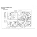
2.2. IC205 (VHiMM3271AN-1Y)
2.2.1 Block Diagram
2.2.2 Pin Connections and short description
Voltage Regulator: 1.0V-REG
47
D/NOT_P
O
MPEG data valid/parity
48
ERROR
O
MPEG packet error
18
AGC_RF
I/O
RF AGC control
(5V tolerant )
17
AGC_IF
I/O
IF AGC control
(5V tolerant )
64
TEST
-
Reserved test mode, must be grounded.
27
GPIO0
I/O
General-purpose input/output port 0.
Reserved test mode,must be ground.
Reserved test mode,must be ground.
49
GPIO1
I/O
General-purpose input/output port 1.
60
GPIO2
I/O
General-purpose input/output port 2 or lock indicator.
59
GPIO3
I/O
General-purpose input/output port 3 or lock indicator.
58
GPIO4
I/O
General-purpose input/output port 4 .
57
GPIO5
I/O
General-purpose input/output port 5.
54
GPIO6
I/O
General-purpose input/output port 6.
53
GPIO7
I/O
General-purpose input/output port 7.
52
GPIO8
I/O
General-purpose input/output port 8.
Resen must be ground.
Resen must be ground.
61
GPIO9
I/O
General-purpose input/output port 9.
23
AUX_CLK
I/O
Auxiliary clock.
25
CS0
I
Chip select LSB.
2, 6, 13, 16
VDDA_2V5
-
Analog power supply (2.5V)
19, 24, 31, 38, 45 ,51, 55, 62
VDD_1V0
-
Digital core supply (1.0V)
22, 28, 34, 41, 50, 56, 63
VDD_3V3
-
Digital I/O supply (3.3V)
Pin
No.
No.
Pin Name
I/O
Pin Function
1
VDD
I
Voltage supply pin
2
GND
-
Ground.
3
CE
I
Output voltage ON/OFF control terminal (When "CE" is "H", Vout is "ON".)
Pin No
Pin Name
I/O
Pin Function
LC-19D1E/S-BK/WH
5 – 6
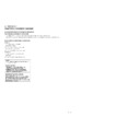
2.3. IC303 (VHiBD5426MU-1Y)
2.3.1 Block Diagram
2.3.2 Pin Connections and short description
STERO-POWER-AMP.
4
NC
-
No Connction
5
VOUT
O
Voltage Output pin with ON/OFF control. (150mA)
Pin No.
Pin Name
I/O
Pin Function
1
BSP2P
I
ch2 The plus side boost strap terminal 2P (Lch+)
2
VCCA
-
Analog system power supply terminal
3
FILP
I
PWM system bias terminal
4
FILA
I
Analog system bias terminal
5
GNDA
-
Analog signal system ground terminal
6
IN2
I
ch2 analog-signal input terminal (Lch+)
7
IN1
I
ch1 analog-signal input terminal (Rch+)
8
PLMT1
I
The voltage and the current conversion terminal 1 for an output power- limitation function
9
PLMT2
I
The voltage and the current conversion terminal 2 for an output power- limitation function
10
PLMT3
I
The voltage and the current conversion terminal 3 for an output power- limitation function
11
PLMT4
I
The voltage and the current conversion terminal 4 for an output power- limitation function
12
BSP1P
I
ch1 The plus side boost strap terminal 1P (Rch+)
13
N.C.
-
No connection
14
VCCP1P
-
ch1 Power supply terminal of the plus side power amplifier output (Rch+)
15
VCCP1P
-
ch1 Power supply terminal of the plus side power amplifier output (Rch+)
16
OUT1P
O
ch1 Plus side PWM signal output terminal (Rch+)
17
OUT1P
O
ch1 Plus side PWM signal output terminal (Rch+)
18
GNDP1
-
ch1 Ground terminal of a power amplifier output (Rch)
19
GNDP1
-
ch1 Ground terminal of a power amplifier output (Rch)
20
OUT1N
O
ch1 Minus side PWM signal output terminal (Rch-)
21
OUT1N
O
ch1 Minus side PWM signal output terminal (Rch-)
22
VCCP1N
-
ch1 Power supply terminal of the minus side power amplifier output (Rch-)
Pin
No.
No.
Pin Name
I/O
Pin Function
LC-19D1E/S-BK/WH
5 – 7
23
VCCP1N
-
ch1 Power supply terminal of the minus side power amplifier output (Rch-)
24
N.C.
-
No connection
25
BSP1N
I
ch1 The minus side boost strap terminal 2N (Rch-)
26
WARNING
O
Warning output terminal . It is a terminal which tells warning of operation.
27
ERROR
O
Error output terminal . It is a terminal which tells an error of operation.
28
MUTEX
I
Audio mute control terminal. (H: mute OFF L: mute ON)
29
N.C.
-
No connection
30
N.C.
-
No connection
31
OSC
I/O
Sampling clock signal input-and-output terminal.
32
MS
I
master slave change terminal (H: slave operation L: master operation)
33
ROSC
I
Sampling clock frequency setting terminal for Insides PWM.
It can usually use it by opening..
It can usually use it by opening..
34
TM
I
Audio mute time constant setting terminal
35
VHOLD
I
The detection voltage setting terminal for a power supply instant cutting detection function
36
BSP2N
I
ch2 Minus side boost strap terminal 2N (Lch-)
37
N.C.
-
No connection
38
VCCP2N
-
ch2 Power supply terminal of the minus side power amplifier output (Lch-)
39
VCCP2N
-
ch2 Power supply terminal of the minus side power amplifier output (Lch-)
40
OUT2N
O
ch2 Minus side PWM signal output terminal (Lch-)
41
OUT2N
O
ch2 Minus side PWM signal output terminal (Lch-)
42
GNDP2
-
ch2 Ground terminal of a power amplifier output. (Lch)
43
GNDP2
-
ch2 Ground terminal of a power amplifier output. (Lch)
44
OUT2P
O
ch2 Plus side PWM signal output terminal (Lch+)
45
OUT2P
O
ch2 Plus side PWM signal output terminal (Lch+)
46
VCCP2P
-
ch2 Power supply terminal of the plus side power amplifier output (Lch+)
47
VCCP2P
-
ch2 Power supply terminal of the plus side power amplifier output (Lch+)
48
N.C.
-
No connection
Pin No.
Pin Name
I/O
Pin Function

