Sharp LC-19D1EWH (serv.man6) Service Manual ▷ View online
LC-19D1E/S-BK/WH
5 – 3
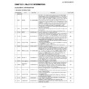
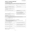
11
IC205
Voltage Regula-
tor: 1.0V-REG
tor: 1.0V-REG
VHIMM3271AN-1Y
This IC is a regulator IC for super-low current consumption that uses
CMOS process. In this Model, this IC generates 1.0V-regurator.
CMOS process. In this Model, this IC generates 1.0V-regurator.
AV
12
IC206
3.3V-REG
VHIPQ1M335M-1Y
This IC can be used for the power regulator circuit up to 0.15A in cur-
rent capacity with the direct current stabilizing supply element that has
the ON/OFF function, the overcurrent protection function, and the over-
heating protection function of the output voltage. In this model, this IC
generates 3.3V-regurator.
rent capacity with the direct current stabilizing supply element that has
the ON/OFF function, the overcurrent protection function, and the over-
heating protection function of the output voltage. In this model, this IC
generates 3.3V-regurator.
AV
13
IC208
Series Regulator:
2.5V-REG
2.5V-REG
VHIBH25FB1G-1Y
This IC is a series regulator of the type with 150mA shutdown. The
overcurrent protection circuit by the output short-circuit etc. and the
overheating protection circuits by the overload etc. are built into this IC.
In this model, this IC generates 2.5V-regurator.
overcurrent protection circuit by the output short-circuit etc. and the
overheating protection circuits by the overload etc. are built into this IC.
In this model, this IC generates 2.5V-regurator.
AV
[INV/POWER UNIT]
1
IC7501
INV-CTL
BD9883FV
BD9883FV is IC for DC-AC inverter control.
POW
[DIGITAL UNIT]
1
IC4001
DIGITAL-PRO-
CESSOR
CESSOR
RH-IXB243WJZZQ
This is a video/audio signal processing IC (Digital Processor) (STi5105)
for digital tuner, which has been manufactured by STMicroelectronics,
and incorporates a CPU. In this equipment, it implements GUI process-
ing and video/audio processing for digital tuner, negotiation processing
with CI-CARD, etc.
for digital tuner, which has been manufactured by STMicroelectronics,
and incorporates a CPU. In this equipment, it implements GUI process-
ing and video/audio processing for digital tuner, negotiation processing
with CI-CARD, etc.
D1
2
IC4201
256Mb-DDR
SDRAM
SDRAM
RH-IXB765WJZZQ
This is a 256Mb DDR SDRAM IC. This IC features a double-data rate
dynamic random-
access memory containing 16M-bits columns by 16 bits.
In this model, it is used for SMI memory (for image processing), and
data is used for operation of the digital processor.
dynamic random-
access memory containing 16M-bits columns by 16 bits.
In this model, it is used for SMI memory (for image processing), and
data is used for operation of the digital processor.
D2
3
IC4202
16M-FLASH
RH-IXC361WJZZQ
This IC is a high performance CMOS super technology 16Mbit Flash
Memory.
Start software (loader) for the CPU with a built-in digital processor and
application software have been written on this Flash Memory.
The digital processor reads these softwares on start-up and implements
them.
Memory.
Start software (loader) for the CPU with a built-in digital processor and
application software have been written on this Flash Memory.
The digital processor reads these softwares on start-up and implements
them.
D2
4
IC4204
64Kb-E2PROM
VHIBR24S64M
BR24S64FVM is 64 Kbits E2PROM for I2C BUS.
This IC stores all data related to the digital module (channels, user set-
tings, etc.).
This IC stores all data related to the digital module (channels, user set-
tings, etc.).
D2
5
IC4205
2.5V_REG
VHIPQ025ENA
This IC generates B2.5V-regurator.
D2
6
IC4401
BUS TRAN-
CEIVER
CEIVER
VHILCX245FT-1Y
This IC is a low voltage (3.3V) CMOS 8bit bidirectional transceiver.
When setting the transmission direction change input DIR to “H”, the A
bus is switched to input and the B bus is changed to output; if the DIR is
set to “L”, the B bus is switched to input and the A bus is changed to
output. When setting the enable input OE to “H”, both A and B buses
enter the high impedance state. In this equipment, it used to switch bus
of the data from CI-CARD.
D3
7
IC4402/
04
04
BUS Buffer
VHILCX16244-1Y
This IC is a CMOS 16-bit bus buffer of a low-voltage drive.
In this model, it is used to control negotiation communication with CI-
CARD.
In this model, it is used to control negotiation communication with CI-
CARD.
D3
8
IC4405
BUS Buffer
VHILCX126FT-1Y
This IC is a three State bus buffer of a low-voltage drive.
In this model, It is used in order to control the negotiation communica-
tion with the serial signal from a digital tuner, and processor IC.
In this model, It is used in order to control the negotiation communica-
tion with the serial signal from a digital tuner, and processor IC.
D3
9
IC4410
5V SW
VHIAOZ1320C-1Y
The AOZ1320 is a P-channel high-side load switch with controlled slew
rate.
In this model, it used as a 5V switch that supplies power to CI_CARD.
rate.
In this model, it used as a 5V switch that supplies power to CI_CARD.
10
IC4601/
02
02
SW-REG(3.3/5V)
VHILV5805M+-1Y
This IC is a 1CH step down switching regulator.
In this model, 3.3V and 5V in a digital unit are generated.
In this model, 3.3V and 5V in a digital unit are generated.
D4
11
IC4603
3CH V-AMP
VHITHS7314D-1Y
This IC is 3CH video amplifier with 6dB amplifier.
In this model, this 6dB video amplifier is used in order to drive the RGB
video signal processed by IC4001 to IC801.
In this model, this 6dB video amplifier is used in order to drive the RGB
video signal processed by IC4001 to IC801.
D4
12
IC4604
1.2V_SERIES-
REG
REG
VHIPQ012GN1-1Y
This IC generates B1.2V-regurator.
D4
13
IC4605
DUAL OP-AMP
VHINJM4565V-1Y
The NJM4565 integrated circuit is a high-gain, wide-bandwidth, dual
low noise operational amplifier capable of driving 20V peak-to-peak into
400
low noise operational amplifier capable of driving 20V peak-to-peak into
400
Ω load.
In this model, it used as a audio pre_amp from IC4001 (digital proces-
sor IC).
sor IC).
D4
NO REF NO
Name
Part Code
Description
Drawing NO
LC-19D1E/S-BK/WH
5 – 4
2. Detailed ICs Information
2.1. IC202 (RH-iXB964WJZZQ) (STV0362)
2.1.1 Block Diagram
2.1.2 Pin Connections and short description
DVB-T RECEIVER
Pin No
Pin Name
I/O
Pin Function
32
NOT_RESET
I
Hardware reset, active Low.
15
XTAL_I
I
Crystal oscillator input/external clock(2.5V)
14
XTAL_O
O
Crystal oscillator output.
1
RF_LEVEL
I
ADC 8 input for RF level monitoring.
3
QP
I
Positive Q analog input for beaseband configuration,
4
QM
I
Nagative Q analog input for baseband configuration.
5
VDDA_ISO
-
Analog ISO neutral polarization.
7
REFP
-
Internal positive reference.
8
REFM
-
Internal negative reference.
9
INCM
-
Internal common mode.
10
IM
I
Negative 1 analog input for IF and baseband configuration.
11
IP
I
Positive 1 analog input for IF and baseband configuration.
12
VDDA_1V0
-
Analog supply (1.0V)
29
SDA
I/O
Serial data (open drain)
30
SCL
I
Serial clock (open drain)
21
SDAT
I/O
SDA tuner (open drain)
20
SCLT
I
SCL tuner.
43
D7
O
Serial MPEG data or parallel MPEG data (bit 7)
42
D6
O
Parallel MPEG data (bit 6)
40
D5
O
Parallel MPEG data (bit 5)
39
D4
O
Parallel MPEG data (bit 4)
37
D3
O
Parallel MPEG data (bit 3)
36
D2
O
Parallel MPEG data (bit 2)
35
D1
O
Parallel MPEG data (bit 1)
33
D0
O
Parallel MPEG data (bit 0)
44
CLK_OUT
O
MPEG byte or bit clock
46
STR_OUT
O
MPEG first byte sync.
LC-19D1E/S-BK/WH
5 – 5
2.2. IC205 (VHiMM3271AN-1Y)
2.2.1 Block Diagram
2.2.2 Pin Connections and short description
Voltage Regulator: 1.0V-REG
47
D/NOT_P
O
MPEG data valid/parity
48
ERROR
O
MPEG packet error
18
AGC_RF
I/O
RF AGC control
(5V tolerant )
17
AGC_IF
I/O
IF AGC control
(5V tolerant )
64
TEST
-
Reserved test mode, must be grounded.
27
GPIO0
I/O
General-purpose input/output port 0.
Reserved test mode,must be ground.
Reserved test mode,must be ground.
49
GPIO1
I/O
General-purpose input/output port 1.
60
GPIO2
I/O
General-purpose input/output port 2 or lock indicator.
59
GPIO3
I/O
General-purpose input/output port 3 or lock indicator.
58
GPIO4
I/O
General-purpose input/output port 4 .
57
GPIO5
I/O
General-purpose input/output port 5.
54
GPIO6
I/O
General-purpose input/output port 6.
53
GPIO7
I/O
General-purpose input/output port 7.
52
GPIO8
I/O
General-purpose input/output port 8.
Resen must be ground.
Resen must be ground.
61
GPIO9
I/O
General-purpose input/output port 9.
23
AUX_CLK
I/O
Auxiliary clock.
25
CS0
I
Chip select LSB.
2, 6, 13, 16
VDDA_2V5
-
Analog power supply (2.5V)
19, 24, 31, 38, 45 ,51, 55, 62
VDD_1V0
-
Digital core supply (1.0V)
22, 28, 34, 41, 50, 56, 63
VDD_3V3
-
Digital I/O supply (3.3V)
Pin
No.
No.
Pin Name
I/O
Pin Function
1
VDD
I
Voltage supply pin
2
GND
-
Ground.
3
CE
I
Output voltage ON/OFF control terminal (When "CE" is "H", Vout is "ON".)
Pin No
Pin Name
I/O
Pin Function
LC-19D1E/S-BK/WH
5 – 6
2.3. IC303 (VHiBD5426MU-1Y)
2.3.1 Block Diagram
2.3.2 Pin Connections and short description
STERO-POWER-AMP.
4
NC
-
No Connction
5
VOUT
O
Voltage Output pin with ON/OFF control. (150mA)
Pin No.
Pin Name
I/O
Pin Function
1
BSP2P
I
ch2 The plus side boost strap terminal 2P (Lch+)
2
VCCA
-
Analog system power supply terminal
3
FILP
I
PWM system bias terminal
4
FILA
I
Analog system bias terminal
5
GNDA
-
Analog signal system ground terminal
6
IN2
I
ch2 analog-signal input terminal (Lch+)
7
IN1
I
ch1 analog-signal input terminal (Rch+)
8
PLMT1
I
The voltage and the current conversion terminal 1 for an output power- limitation function
9
PLMT2
I
The voltage and the current conversion terminal 2 for an output power- limitation function
10
PLMT3
I
The voltage and the current conversion terminal 3 for an output power- limitation function
11
PLMT4
I
The voltage and the current conversion terminal 4 for an output power- limitation function
12
BSP1P
I
ch1 The plus side boost strap terminal 1P (Rch+)
13
N.C.
-
No connection
14
VCCP1P
-
ch1 Power supply terminal of the plus side power amplifier output (Rch+)
15
VCCP1P
-
ch1 Power supply terminal of the plus side power amplifier output (Rch+)
16
OUT1P
O
ch1 Plus side PWM signal output terminal (Rch+)
17
OUT1P
O
ch1 Plus side PWM signal output terminal (Rch+)
18
GNDP1
-
ch1 Ground terminal of a power amplifier output (Rch)
19
GNDP1
-
ch1 Ground terminal of a power amplifier output (Rch)
20
OUT1N
O
ch1 Minus side PWM signal output terminal (Rch-)
21
OUT1N
O
ch1 Minus side PWM signal output terminal (Rch-)
22
VCCP1N
-
ch1 Power supply terminal of the minus side power amplifier output (Rch-)
Pin
No.
No.
Pin Name
I/O
Pin Function

