Sharp 28JW-73H (serv.man12) Service Manual ▷ View online
-:+
5
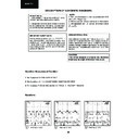
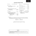
ELECTRICAL CHARACTERISTICS
(refer to Figure 1 on page 3)
Tamb = 25
°
C unless otherwise specified, Vcc =
±
12V, f
vert
=50Hz
Note: 1
Input voltage = 0, measured after the filter (e.g. accross the 470 nF filter capacitor)
Note: 2
Supply rejection of the positive or negative power supply. Vcc ripple =1Vpp, f=100Hz, measured on the sense
resistor.
resistor.
Note: 3
Power dissipated in the circuit in the case of the application from Figure 1 and the current in the deflection
yoke adjusted to 2.5App. The corresponding power dissipated in the vertical deflection yoke is 2.8W.
yoke adjusted to 2.5App. The corresponding power dissipated in the vertical deflection yoke is 2.8W.
Symbol
Parameter
Test Conditions
Min.
Typ.
Max.
Units
+Vcc
Positive supply range
+10
+18
V
-Vcc
Negative supply range
-18
-10
V
∆
Vcc
Maximum recommended difference
between +Vcc and
between +Vcc and
±
4
V
Vcc
start
Low Vcc detection
±
6.5
V
Iq
Quiescent supply current
Input voltage = 0
14
mA
Iy
Maximum recommended vertical
yoke current
yoke current
±
1.25
A
I
13
, I
12
Amplifier Input bias current
-0.1
µ
A
V
OS
Output Offset voltage
Note 1
-50
+50
mV
SVR
Supply voltage rejection
Note 2
82
dB
Fly
thr
Flyback detection threshold
(positive slope)
(positive slope)
V(14)
1.5
V
Fly
thf
Flyback detection threshold
(negative slope)
(negative slope)
V(14)
0.5
V
Pd
Integrated circuit
Dissipated power
Dissipated power
Note 3
1.1
W
Fsw
Switching frequency
R
freq
= 10k
Ω
120
140
160
kHz
Fsw - op
Switching frequency operative range
100
200
kHz
R
freq
Frequency controller resistor range
Pin 10
7
10
14
k
Ω
Vcc
–
679,&
Figure
1.
Test
Test
and
Application
Cir
cuit
Flyback
Flyback
Output
Modulator
+
_
drive
generator
detection
+VCC
+VCC power
CFLYBACK
CFLY+
100nF
VREG
IN+
IN -
1k
Ω
10k
Ω
EA out
-VCC power
-VCC
-VCC
BOOT
Cboot
470nF
10k
Ω
4.7nF
FREQ
FEEDCAP
SGND
Pins 1,2,3,18,19,20
OUT
0.5
Ω
Deflect.
Yoke*
CFLY-
+VCC
1mH
Input signal
1k
Ω
220nF
-VCC
100nF
100nF
1000
µ
F
1000
µ
F
STV9380
100
µ
F
14
11
9
17
560pF
150
Ω
200
Ω
15
16
8
TDA9380
5
6
7
4
13
12
150
Ω
10
Vref
-VCC
470pF
* Deflection yoke characteristics: R = 5.5
Ω
, L = 7mH
100nF
Sense
resistor
f
vert
= 50Hz
-:+
7($,&
%ORFN'LDJUDP
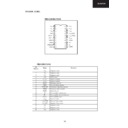
PINNING
SYMBOL PIN
DESCRIPTION
V
CC
1
supply voltage
GND
2
ground
CTRL
3
control input
DEM
4
input from auxiliary winding for
demagnetization timing, OVP and OPP
demagnetization timing, OVP and OPP
I
sense
5
programmable current sense input
DRIVER
6
gate driver output
HVS
7
high voltage safety spacer, not
connected
connected
DRAIN
8
drain of external MOS switch, input for
start-up current and valley sensing
start-up current and valley sensing
handbook, halfpage
MGU231
TEA1507
1
2
3
4
VCC
GND
CTRL
DEM
DRAIN
HVS
DRIVER
Isense
8
7
6
5
Fig.3 Pin configuration.
h
SUPPLY
MANAGEMENT
internal
supply
UVLO
start
M-level
VCC
1
2
3
GND
S1
CTRL
FREQUENCY
CONTROL
VOLTAGE
CONTROLLED
OSCILLATOR
LOGIC
LOGIC
OVER-
VOLTAGE
PROTECTION
OVERPOWER
PROTECTION
PROTECTION
short
winding
soft
start
S2
OVER-
TEMPERATURE
PROTECTION
S
Q
R
UVLO
Q
MAXIMUM
ON-TIME
PROTECTION
POWER-ON
RESET
−
1
VALLEY
TEA1507
100 mV
clamp
DRIVER
START-UP
CURRENT SOURCE
0.75 V
0.5 V
5
Isense
6
DRIVER
MGU230
4
DEM
8
DRAIN
7
HVS
n.c.
n.c.
OCP
LEB
blank
Iss
2.5 V
burst
detect
detect
-:+
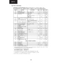
CHARACTERISTICS
T
T
amb
= 25
°
C; V
CC
= 15 V; all voltages are measured with respect to ground (pin 2); currents are positive when flowing
into the IC; unless otherwise specified.
SYMBOL
PARAMETER
CONDITIONS
MIN.
TYP.
MAX. UNIT
Start-up current source (pin 8)
I
i(DRAIN)
supply current drawn from drain pin
V
CC
= 0 V; V
DRAIN
> 100 V
1.0
1.2
1.4
mA
with auxiliary supply;
V
V
DRAIN
> 100 V
−
100
300
µ
A
BV
DSS
breakdown voltage
650
−
−
V
M-level
mains-dependent operation-enabling level
60
−
100
V
V
CC
management (pin 1)
V
CC(start)
start-up voltage on V
CC
10.3
11
11.7
V
V
CC(UVLO)
under voltage lock-out on V
CC
8.1
8.7
9.3
V
V
CC(hys)
hysteresis voltage on V
CC
V
CC(start)
−
V
CC(UVLO)
2.0
2.3
2.6
V
I
i(VCC)H
pin V
CC
charging current
V
DRAIN
> 100 V; V
CC
< 3V
−
1.2
−
1
−
0.8
mA
I
i(VCC)L
pin V
CC
charging current
V
DRAIN
> 100 V;
3 V < V
CC
< V
CC(UVLO)
−
1.2
−
0.75
−
0.45 mA
I
VCC(restart)
pin V
CC
restart current
V
DRAIN
> 100 V;
V
CC(UVLO)
< V
CC
< V
CC(start)
−
650
−
550
−
450
µ
A
I
CC(operate)
supply current under normal operation
no load on pin DRIVER
1.1
1.3
1.5
mA
Demagnetization management (pin 4)
V
DEM
demagnetization comparator threshold
voltage on pin DEM
voltage on pin DEM
50
100
150
mV
I
DEM
pin DEM current
V
DEM
= 50 mV
−
50
(1)
−
0
nA
V
clamp(DEM)(neg)
negative clamp voltage on pin DEM
at I
DEM
=
−
150
µ
A
−
0.5
−
0.25
−
0.05 V
V
clamp(DEM)(pos)
positive clamp voltage on pin DEM
at I
DEM
= 250
µ
A
0.5
0.7
0.9
V
t
suppr
suppression of transformer ringing at start
of secondary stroke
of secondary stroke
1.1
1.5
1.9
µ
s
Pulse width modulator
t
on(min)
minimum on-time
−
t
leb
−
ns
t
on(max)
maximum on-time
latched
40
50
60
µ
s
Oscillator
f
oscL
oscillator low frequency (fixed frequency)
V
CTRL
> 1.5 V
5
6.5
8
kHz
f
oscH
oscillator high frequency (fixed frequency) V
CTRL
< 1 V
145
175
205
kHz
V
vco(start)
peak voltage at pin I
sense
, where
frequency reduction starts
see Fig.6
−
75
−
mV
V
vco(max)
peak voltage at pin I
sense
, where the
frequency is equal to f
oscL
−
50
−
mV
Duty cycle control (pin 3)
V
CTRL(min)
min. voltage on CTRL (max. duty cycle)
−
1.0
−
V
V
CTRL(max)
max. voltage on CTRL (min. duty cycle)
−
1.5
−
V
7($,&
-:+
7($,&
Note
1. Guaranteed by design.
Burst mode standby (pin 3)
V
th(burst)(on)
burst mode standby active threshold
voltage
voltage
at I
burst
= 6 mA
3.3
3.8
4.3
V
I
th(burst)(on)
burst mode standby active current
16
−
−
mA
I
th(burst)(off)
burst mode standby inactive current
−
−
6
mA
t
(burst-blank)
burst mode standby blanking time
25
30
35
µ
s
Valley switch (pin 8)
∆
V/
∆
t
valley
∆
V/
∆
t for valley recognition
−
85
−
+
85
V/
µ
s
t
valley-swon
delay from valley recognition to switch-on
−
150
(1)
−
ns
Current and short winding protection (pin 5)
V
sense(max)
maximum source voltage OCP
∆
V/
∆
t = 0.1 V/
µ
s
0.48
0.52
0.56
V
t
propagation
delay from detecting V
sense(max)
to
switch-off
∆
V/
∆
t = 0.5 V/
µ
s
−
140
185
ns
V
swp
short winding protection voltage
0.83
0.88
0.96
V
t
leb
blanking time for current and short
winding protection
winding protection
300
370
440
ns
I
ss
soft start current
V
sense
< 0.5 V
45
60
75
µ
A
Overvoltage protection (pin 4)
I
(OVP)(DEM)
OVP protection level at pin 4, set by the
demagnetization resistor R
demagnetization resistor R
DEM
; see
Section “OverVoltage Protection (OVP)”
54
60
66
µ
A
Overpower protection (pin 4)
I
(OPP)(DEM)
OPP current at pin 4, start of OPP
correction. Set by the demagnetization
resistor R
correction. Set by the demagnetization
resistor R
DEM
; see Section “OverPower
Protection (OPP)”
−
−
24
−
µ
A
I
(OPP50%)(DEM)
OPP current at pin 4 where maximum
source voltage is limited to 0.3 V
source voltage is limited to 0.3 V
−
−
100
−
µ
A
Driver (pin 6)
I
source
source current capability of driver
V
CC
= 9.5 V; V
DRIVER
= 2 V
−
−
170
−
88
mA
I
sink
sink current capability of driver
V
CC
= 9.5 V; V
DRIVER
= 2 V
−
300
−
mA
V
CC
= 9.5 V;
V
DRIVER
= 9.5 V
400
700
−
mA
V
o(driver)(max)
maximum output voltage of the driver
V
CC
> 12 V
−
11.5
12
V
Temperature protection
T
prot(max)
maximum temperature threshold
130
140
150
°
C
T
prot(hyst)
hysteresis temperature
−
8
(1)
−
°
C
SYMBOL
PARAMETER
CONDITIONS
MIN.
TYP.
MAX. UNIT
Display

