Sharp AM-300 (serv.man5) Service Manual ▷ View online
AM-300DE
5 – 1
AM-300DE
Service Manual
CHAPTER 5.
CIRCUIT DESCRIPTION
[1] Circuit description
1. General description
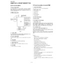
The compact design of the control PWB is obtained by using MFP
ASIC OA-2000 in the main control section and high density printing of
surface mounting parts. Each PWB is independent according to its
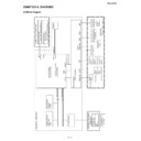
function as shown in Fig. 1.
ASIC OA-2000 in the main control section and high density printing of
surface mounting parts. Each PWB is independent according to its
function as shown in Fig. 1.
2. PWB configuration
2.1. Control PWB
The control PWB controls peripheral PWBs, mechanical parts, trans-
mission, and performs overall control of the unit.
mission, and performs overall control of the unit.
2.2. Power supply PWB
This PWB provides voltages of +3.3V, +5V and +24V to the another
PWB.
PWB.
2.3. Panel PWB
The panel PWB allows input of the operation keys.
2.4. High voltage PWB
This PWB provides the high voltage to printer process units.
2.5. LCD PWB
This PWB controls the LCD display.
[2] Circuit description of control PWB
1. General description
The control PWB is composed of the following blocks..
1.1. Main control block
1) Controller block
2) Memory block
3) Speaker block
4) Scanner I/F block
5) Panel I/F block
1.2. Printer control block
1.3. Power section
2. Description of each block
2.1. Main control block
Main control block consisting of CPU OA-2000 with 32bit microproces-
sor core, SDRAM (128Mbit), FLASH (16Mbit), FAX MODEM, etc., con-
trols scanning, images processing, FAX communication, user
interface, USB interface etc., that is all except for printer controlling.
sor core, SDRAM (128Mbit), FLASH (16Mbit), FAX MODEM, etc., con-
trols scanning, images processing, FAX communication, user
interface, USB interface etc., that is all except for printer controlling.
2.1.1 Controller block
1) OA-2000 (IC1): pin-208 QFP (Main CPU)
1) OA-2000 (IC1): pin-208 QFP (Main CPU)
This is a microcomputer with 32bit microprocessor (ARC) core, which
periphery functions are integrated into.
periphery functions are integrated into.
This device is equipped with the following function. The clock inputs
24MHz from outside and operates at 4-times frequency (96MHz) inter-
nally.
24MHz from outside and operates at 4-times frequency (96MHz) inter-
nally.
Feature
• SDRAM Controller
Addressing, Control and Refresh to SDRAM (IC4)
• USB 2.0 Client I/F (High Speed & Full Speed)
Connection for PC
• General Purpose I/O port
Controlling Panel, LIU, Motor driver, etc.
Inputting of each sensor and status signals
• Contact Image Sensor I/F and Analog Front End
Processing of SCAN video signal and its A/D conversion.
• Hardware Image Processing Accelerators
• JBIG & JPEG Hardware Image Compression and Decompression
• Serial communication I/F
Communicating with Printer CPU (IC21)
• Peripheral Bus I/F
FAX MODEM (IC18) and KEY & STATUS signal buffer (IC10) is
connected via Peripheral Bus.
connected via Peripheral Bus.
• Pulse Width Modulators
This generates key input sound, alarm sound and ringer sound.
• Real Time Clock Generator
It is oscillated with quartz oscillator of 32.768kHz and the clock is
provided.
provided.
Fig. 1
HEATER
LAMP
AC CORD
OPERATION
PANEL PWB
CIS
LCD
SCANNER
MOTOR
FAN
OPTICAL UNIT (LSU)
ROLLER SENSOR
MAIN MOTOR
PICKUP MOTOR
TONER C/T SENSOR
FUSING UNIT
THERMISTOR
SPEAKER
CONTROL
PWB
POWER
SUPPLY
PWB
HIGH VOLTAGE PWB
AM-300DE
5 – 2
OA-2000 (IC1) Terminal description (1/4)
No.
Pin name
I/O
Pin Description
1
GP_L6
Bidirectional
General Purpose IO
2
GP_L7
Bidirectional
General Purpose IO
3
GP_M0
Bidirectional
General Purpose IO
4
GP_M1
Bidirectional
General Purpose IO
5
GP_M2
Bidirectional
General Purpose IO
6
GP_M3
Bidirectional
General Purpose IO
7
GP_M4
Bidirectional
General Purpose IO
8
GP_M5/UA1_RX_DATA
Bidirectional
General Purpose IO/Serial Communication Interface(Receiving data)
9
GP_M6/UA1_SCLK
Bidirectional
General Purpose IO/Serial Communication Interface(Serial clock)
10
VSS
GND digital
Ground
11
CORE_VDD18
+1.8V digital
Power
12
GP_M7/UA1_TX_DATA
Bidirectional
General Purpose IO/Serial Communication Interface(Sending data)
13
GP_N0/PB_CS0
Bidirectional
General Purpose IO/Peripheral Bus Chip Select 0
14
GP_N1
Bidirectional
General Purpose IO
15
IO_VDD33
+3.3V digital
Power
16
GP_N2
Bidirectional
General Purpose IO
17
GP_N3/PB_CS3
Bidirectional
General Purpose IO/Peripheral Bus Chip Select 3
18
GP_N4/PB_NOE
Bidirectional
General Purpose IO/Peripheral Bus Output Enable
19
GP_N5/PB_NWE
Bidirectional
General Purpose IO/Peripheral Bus Write Enable
20
GP_O0/PB_ADDR0
Bidirectional
General Purpose IO/Peripheral Bus Address
21
GP_O1/PB_ADDR1
Bidirectional
General Purpose IO/Peripheral Bus Address
22
VSS
GND digital
Ground
23
GP_O2/PB_ADDR2
Bidirectional
General Purpose IO/Peripheral Bus Address
24
GP_O3/PB_ADDR3
Bidirectional
General Purpose IO/Peripheral Bus Address
25
GP_O4/PB_ADDR4
Bidirectional
General Purpose IO/Peripheral Bus Address
26
GP_O5
Bidirectional
General Purpose IO
27
GP_O6
Bidirectional
General Purpose IO
28
GP_O7
Bidirectional
General Purpose IO
29
GP_P0/PB_DATA0
Bidirectional
General Purpose IO/Peripheral Bus Data
30
GP_P1/PB_DATA1
Bidirectional
General Purpose IO/Peripheral Bus Data
31
IO_VDD33
+3.3V digital
Power
32
GP_P2/PB_DATA2
Bidirectional
General Purpose IO/Peripheral Bus Data
33
GP_P3/PB_DATA3
Bidirectional
General Purpose IO/Peripheral Bus Data
34
GP_P4/PB_DATA4
Bidirectional
General Purpose IO/Peripheral Bus Data
35
GP_P5/PB_DATA5
Bidirectional
General Purpose IO/Peripheral Bus Data
36
GP_P6/PB_DATA6
Bidirectional
General Purpose IO/Peripheral Bus Data
37
GP_P7/PB_DATA7
Bidirectional
General Purpose IO/Peripheral Bus Data
38
VSS
GND digital
Ground
39
CORE_VDD18
+1.8V digital
Power
40
IO_VDD33
+3.3V digital
Power
41
ADC_AVSS
GND analog
Ground
42
ADC_VIN0
Input analog
A/D Converter Input 0
43
ADC_VIN1
Input analog
A/D Converter Input 1
44
ADC_VIN2
Input analog
A/D Converter Input 2
45
ADC_VIN3
Input analog
A/D Converter Input 3
46
ADC_AVDD33
+3.3V analog
Power
47
ADC_VIN4
Input analog
A/D Converter Input 4
48
ADC_VIN5
Input analog
A/D Converter Input 5
49
ADC_VIN6
Input analog
A/D Converter Input 6
50
ADC_VIN7
Input analog
A/D Converter Input 7
51
ADC_AVSS
GND analog
Ground
52
IO_VDD33
+3.3V digital
Power
53
IO_VDD33
+3.3V digital
Power
54
GP_C0
Bidirectional
General Purpose IO
55
GP_D0
Bidirectional
General Purpose IO
56
GP_C1
Bidirectional
General Purpose IO
57
GP_D1
Bidirectional
General Purpose IO
58
GP_C2
Bidirectional
General Purpose IO
59
GP_C3
Bidirectional
General Purpose IO
60
IO_VDD33
+3.3V digital
Power
61
GP_C4
Bidirectional
General Purpose IO
62
GP_C5
Bidirectional
General Purpose IO
63
GP_C6
Bidirectional
General Purpose IO
64
GP_C7
Bidirectional
General Purpose IO
AM-300DE
5 – 3
OA-2000 (IC1) Terminal description (2/4)
No.
Pin name
I/O
Pin Description
65
CORE_VDD18
+1.8V digital
Power
66
VSS
GND digital
Ground
67
GP_F0/PO_PAGE_SYNC
Bidirectional
General Purpose IO/Print Page Synchronous Input
68
GP_F1/PO_LINE_SYNC
Bidirectional
General Purpose IO/Print Line Synchronous Input
69
GP_F2
Bidirectional
General Purpose IO
70
GP_F3
Bidirectional
General Purpose IO
71
IO_VDD33
+3.3V digital
Power
72
GP_F4
Bidirectional
General Purpose IO
73
GP_F5
Bidirectional
General Purpose IO
74
GP_F6
GND digital
General Purpose IO
75
GP_F7
+1.8V digital
General Purpose IO
76
VSS
GND digital
Ground
77
ROM_CS_L
Output
ROM Chip Select
78
SDRAM_DATA0
Bidirectional
SDRAM Data Bus
79
IO_VDD33
+3.3V digital
Power
80
SDRAM_DATA1
Bidirectional
SDRAM Data Bus
81
SDRAM_DATA2
Bidirectional
SDRAM Data Bus
82
SDRAM_DATA3
Bidirectional
SDRAM Data Bus
83
SDRAM_DATA4
Bidirectional
SDRAM Data Bus
84
CORE_VDD18
+1.8V digital
Power
85
VSS
GND digital
Ground
86
SDRAM_DATA5
Bidirectional
SDRAM Data Bus
87
SDRAM_DATA6
Bidirectional
SDRAM Data Bus
88
SDRAM_DATA7
Bidirectional
SDRAM Data Bus
89
SDRAM_DATA8
Bidirectional
SDRAM Data Bus
90
IO_VDD33
+3.3V digital
Power
91
SDRAM_DATA9
Bidirectional
SDRAM Data Bus
92
SDRAM_DATA10
Bidirectional
SDRAM Data Bus
93
SDRAM_DATA11
Bidirectional
SDRAM Data Bus
94
SDRAM_DATA12
Bidirectional
SDRAM Data Bus
95
VSS
GND digital
Ground
96
SDRAM_DATA13
Bidirectional
SDRAM Data Bus
97
SDRAM_DATA14
Bidirectional
SDRAM Data Bus
98
SDRAM_DATA15
Bidirectional
SDRAM Data Bus
99
SDRAM_DQMA0
Output
SDRAM IO Mask
100
IO_VDD33
+3.3V digital
Power
101
SDRAM_DQMA1
Output
SDRAM IO Mask
102
SDRAM_CS0_L
Output
SDRAM Chip Select 0
103
SDRAM_CKE
Output
SDRAM Clock Enable
104
SDRAM_CLK
Output
SDRAM Clock
105
VSS
GND digital
Ground
106
SDRAM_ADDR12
Bidirectional
SDRAM Address Bus
107
SDRAM_ADDR11
Bidirectional
SDRAM Address Bus
108
SDRAM_ADDR10
Bidirectional
SDRAM Address Bus
109
SDRAM_ADDR9
Bidirectional
SDRAM Address Bus
110
IO_VDD33
+3.3V digital
Power
111
SDRAM_ADDR8
Bidirectional
SDRAM Address Bus
112
SDRAM_ADDR7
Bidirectional
SDRAM Address Bus
113
SDRAM_ADDR6
Bidirectional
SDRAM Address Bus
114
SDRAM_ADDR5
Bidirectional
SDRAM Address Bus
115
VSS
GND digital
Ground
116
SDRAM_ADDR4
Bidirectional
SDRAM Address Bus
117
IO_VDD33
+3.3V digital
Power
118
SDRAM_CS1A_L
Output
SDRAM Chip Select 1
119
SDRAM_ADDR3
Bidirectional
SDRAM Address Bus
120
CORE_VDD18
+1.8V digital
Power
121
VSS
GND digital
Ground
122
SDRAM_ADDR2
Bidirectional
SDRAM Address Bus
123
SDRAM_ADDR1
Bidirectional
SDRAM Address Bus
124
SDRAM_ADDR0
Bidirectional
SDRAM Address Bus
125
SDRAM_BA1
Bidirectional
SDRAM Bank Select Address
126
IO_VDD33
+3.3V digital
Power
127
SDRAM_BA0
Bidirectional
SDRAM Bank Select Address
128
SDRAM_RAS_L
Bidirectional
SDRAM Row Address Strobe Command
AM-300DE
5 – 4
OA-2000 (IC1) Terminal description (3/4)
No.
Pin name
I/O
Pin Description
129
SDRAM_CAS_L
Bidirectional
SDRAM Column Address Strobe Command
130
SDRAM_WE_L
Bidirectional
SDRAM Write Enable
131
VSS
GND digital
Ground
132
GP_H0/PI_TGEN0
Bidirectional
General Purpose IO/Timing Generator for CIS
133
GP_H1/BASE_CLK
Bidirectional
General Purpose IO/Base Clock Input
134
GP_H2/PI_TGEN2
Bidirectional
General Purpose IO/Timing Generator for CIS
135
GP_H3
Bidirectional
General Purpose IO
136
IO_VDD33
+3.3V digital
Power
137
RTC_VSS
GND digital
Ground
138
RTC_XIN
Crystal/Input
Real Time Clock Crystal
139
RTC_XOUT
Crystal
Real Time Clock Crystal
140
RTC_VDD18
+1.8V digital
Real Time Clock Power
141
VSS
GND digital
Ground
142
CORE_VDD18
+1.8V digital
General Purpose IO
143
GP_H4
Bidirectional
Power
144
GP_H5/PI_TGEN5
Bidirectional
General Purpose IO/Timing Generator
145
GP_H6/PI_TGEN6
Bidirectional
General Purpose IO/Timing Generator
146
GP_H7/PI_TR_TGEN
Bidirectional
General Purpose IO/Timing Generator
147
IO_VDD33
+3.3V digital
Power
148
GP_J0
Bidirectional
General Purpose IO
149
GP_J1
Bidirectional
General Purpose IO
150
GP_J2
Bidirectional
General Purpose IO
151
GP_J3
Bidirectional
General Purpose IO
152
VSS
GND digital
Ground
153
GP_J4
Bidirectional
General Purpose IO
154
GP_J5
Bidirectional
General Purpose IO
155
GP_J6
Bidirectional
General Purpose IO
156
GP_J7
Bidirectional
General Purpose IO
157
IO_VDD33
+3.3V digital
Power
158
GP_K0/PI_TGEN_AUX
Bidirectional
General Purpose IO/Timing Generator
159
GP_K1
Bidirectional
General Purpose IO
160
VSS
GND digital
Ground
161
RESET_L
Bidirectional
Reset signal Input
162
AFE_VINB
Input analog
AFE Video Input
163
AFE_VING
Input analog
AFE Video Input
164
AFE_ANAREF
GND analog
AFE Reference Voltage Input
165
AFE_VINR
Input analog
AFE Video Input
166
AFE_AVSS
GND analog
Ground
167
AFE_VREFN
Analog
AFE Reference Voltage Input
168
AFE_VREFP
Analog
AFE Reference Voltage Input
169
AFE_VCM
Analog
AFE Reference Voltage Input
170
AFE_AVDD33
+3.3 V analog
Power
171
VSS
GND digital
Ground
172
CORE_VDD18
+1.8V digital
Power
173
TCK
Input
(Used only debug mode)
174
TMS
Input
(Used only debug mode)
175
TDI
Input
(Used only debug mode)
176
TDO
Output
(Used only debug mode)
177
CK_PWM1
Bidirectional
Pulse Width Modulators
178
CK_PWM0
Bidirectional
Pulse Width Modulators
179
IO_VDD33
+3.3V digital
Power
180
XOUT
Crystal
Crystal
181
XIN
Crystal/Input
Crystal
182
VSS
GND digital
Ground
183
CORE_VDD18
+1.8V digital
Power
184
PLL_AVDD18
+1.8V analog
Power
185
PLL_AVSS
GND digital
Ground
186
HOST1_DM
Bidir.analog
USB Host Interface
187
HOST1_DP
Bidir.analog
USB Host Interface
188
HOST_AVDD33
+3.3V analog
Power
189
HOST0_DM
Bidir.analog
USB Host Interface
190
HOST0_DP
Bidir.analog
USB Host Interface
191
HOST_AVSS
GND analog
Ground
192
DEV_RSDM
Output analog
USB Device Interface

