Sharp LL-T1610W (serv.man7) Service Manual ▷ View online
CHAPTER 5. HARDWARE
[1] System description
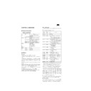
1. Hardware specification
Item
Description
CPU
incorporated in PW164 (80186
compatible)
compatible)
CPU clock speed 43.2 MHz
Memory
RAM
32 KByte DRAM is incorporated in
PW164
PW164
Flash memory
NOR type flash with 1Mbyte boot
block, 8Mb x 1:16-bit bus
block, 8Mb x 1:16-bit bus
E
2
PROM (DATA) 16 Kbit E
2
PROM (I
2
C control)
E
2
PROM (DDC)
1Kbit E
2
PROM (DD1/DDC2B) x 2
Scaler
PW164-20R
MCLK: 129.6 MHz
DCLK: 108 MHz
MCLK: 129.6 MHz
DCLK: 108 MHz
AD
converter
converter
ADC9884ASK-140
TMDS
Receiver
SiI151A
USB
USB hub
uPD72012
USB switch
uPD16875
[2] PW164
2-1. CPU
The PW164 incorporates an 80186-compatible CPU.
The CPU incorporates 32-Kbyte RAM in addition to peripheral de-
vices.
vices.
The CPU directly controls the following memory and I/O: built-in RAM,
flash memory, built-in peripheral devices, scaler-contained 10 regis-
ters. The other devices are controlled from the general port through
the I
flash memory, built-in peripheral devices, scaler-contained 10 regis-
ters. The other devices are controlled from the general port through
the I
2
C bus.
The memory space of the CPU is equal to the capacity of the flash
memory.
memory.
Allocated on the memory space are flash memory, main memory,
PW164-incorporated I/Os, external chip select. You cannot access to
the area of flash memory with which these spaces overlap.
PW164-incorporated I/Os, external chip select. You cannot access to
the area of flash memory with which these spaces overlap.
The clock speed of the CPU is 43.2 MHz (14.4 MHz in the power
save mode).
save mode).
2-2. Peripheral device incorporated in the CPU
The PW164 incorporates general I/O ports (16 bits), timer (2 ch +
watchdog), interrupt controller, UART, and IR decoder.
watchdog), interrupt controller, UART, and IR decoder.
2-2-1. General ports
The PW164 incorporates 16-bit I/O ports which can be set for every
bit.
bit.
Here are applications of the general ports .
CPU port
Signal
name
I/O
Function
PORTA0
SDA
I/O
I
2
C data
PORTA1
SCL
I/O
I
2
C clock
PORTA2
BOOTWE
O
Write protects flash memory BOOT
area
area
0: Write to BOOT area is prohibited.
1: Write to BOOT area is allowed.
1: Write to BOOT area is allowed.
PORTA3
VPPEN
O
Write protects flash memory
0: Write to flash memory is prohibited.
1: Write to flash memory is allowed.
1: Write to flash memory is allowed.
PORTA4
CLKEN
O
Selects clock (MCK, DCK) frequency.
0: Low speed (power save)
1: Normal speed (during operation)
1: Normal speed (during operation)
PORTA5
LCDON
O
Controls LCD power
0: LCD, TMDS off
1: LCD, TMDS on
1: LCD, TMDS on
PORTA6
XVPWDN
O
Controls ADC power
0: ADC on
1: ADC off
1: ADC off
PORTA7
TMDSON
O
Controls SiI151A power
0: TMDS off
1: TMDS on
1: TMDS on
PORTB0
MENU
I
Menu key input 0: Key input
PORTB1
SELECT
I
Select key input 0: Key input
PORTB2
+
I
Left arrow key input 0: Key input
PORTB3
-
I
Right arrow key input 0: Key input
PORTB4
INPUT
I
Input select key input 0: Key input
PORTB5
SCDT
I
Detects DVI data input
PORTB6
DPMS
O
Selects V and H in DPMS mode
0: Analog V, H
1: Digital V, H
1: Digital V, H
PORTB7
T5V
O
Detects DVI 5 V
The devices not assigned on the CPU’s map are controlled by the I
2
C
interface which uses PORTA0 and PORTA1 of the general port.
The I
2
C is a 2-wire type directional serial interface. The device ad-
dress from the host determines which device should be activated.
The addresses for devices connected to the I
2
C are as follows:
Part name
Type
A6 A5 A4 A3
A2
A1 A0
Read
address
Write
address
AD9884A
ADC
1
0
0
1
1
0
1
9BH
9AH
HN58X2416 16K
E
2
PROM
1
0
1
0
a10 a9 a8
AXH
AXH
M62334FP
DA
Converter
Converter
1
0
0
1
1
0
0
99H
98H
: a10, a9, and a8 are memory addresses.
For more information about the I
2
C, refer to each device’s instruction
manual and the guide book about the I
2
C published by Phillips.
BOOTWE and VPPEN
The BOOTWE signal can be connected to flash memory on the PWB.
When this signal is connected flash memory, it becomes possible to
control the #WP of flash memory on the PWB by software (it is
control the #WP of flash memory on the PWB by software (it is
possible to rewrite the boot area).
The VPPEN signal is used to mask the WE signal of flash memory,
instead of controls the VPP of flash memory (VPP is always applied).
instead of controls the VPP of flash memory (VPP is always applied).
Therefore, when the VPPEN is at low level, data cannot be written to
flash memory and no command is issued.
flash memory and no command is issued.
2-2-2. IR decoder
The IR decoder of the PW164 has 2 lines of input.
This model does not use the IR decoder.
2-3. Scaler engine
On the PW164, the DCK is 108 MHz and MCK is 129.6 MHz.
[3] AD9884A
The AD9884A converts the analog RGB output from the PC to digital
48-bit data and outputs it to the PW164.
48-bit data and outputs it to the PW164.
Data from the PC is compatible with a dot clock of up to 140 MHz.
The AD 9884A can receive up to 75 MHz (dot clock of 135 MHz) at
SXGA.
The AD 9884A can receive up to 75 MHz (dot clock of 135 MHz) at
SXGA.
The AD9884A is controlled by the I
2
C (slave address 9AH/9BH).
In the power save mode including the DPMS mode, the AD9884A is
put in the power-down mode by the XVPWDN signal (general port of
the PW164).
put in the power-down mode by the XVPWDN signal (general port of
the PW164).
The AD9884A is connected to the PW164 with the dual channel
mode (48 bits).
mode (48 bits).
[4] SiI151A
The SiI151A converts serial data outputted from the PC into digital
48-bit data and then outputs it to the PW164.
48-bit data and then outputs it to the PW164.
In the power save mode including the DPMS mode, the SiI151A is
put in the power-down mode by the TMDSON signal (general port of
the PW164).
put in the power-down mode by the TMDSON signal (general port of
the PW164).
There is no software-controlled item other than the power-down
mode.
mode.
[5] LH28F800BVE
For the program ROM, an 8-Mbit flash memory LH28F800BVE is
used. The LH28F800BVE consists of two 4K-word boot block, six
4K-word parameter block and 15 32K-word main block.
used. The LH28F800BVE consists of two 4K-word boot block, six
4K-word parameter block and 15 32K-word main block.
Put the VPPEN signal (PW164 general port) in High level before
issuing the command or writing data to flash memory.
issuing the command or writing data to flash memory.
[6] HN58X2416
A 16-Kbit E
2
PROM HN58x2416 is used for storing data such as user
information.
The HN58x2416 uses I
2
C for reading and writing data.
The slave addresses for the HN58x2416 are A0H - AFH and they
need to be changed according to memory addresses which data is
read from or written to.
need to be changed according to memory addresses which data is
read from or written to.
The WP (write protect) pin of the HN58x2416 is not used and thus it
is possible to rewrite all areas.
is possible to rewrite all areas.
[7] M62334
The M62334, a 4-channel, 8-bit DA converter which is controlled by
the I
the I
2
C, controls the backlight and LED. (slave addresses 98H/99H).
The output of the M62334 is set as follows:
D7
D6
D5
D4
D3
D2
D1
D0
M62334 output
0
0
0
0
0
0
0
0
Vcc/256 1
0
0
0
0
0
0
0
1
Vcc/256: 2
0
0
0
0
0
0
1
0
Vcc/256 3
...
...
...
...
...
...
...
...
...
1
1
1
1
1
1
1
0
Vcc/256 255
1
1
1
1
1
1
1
1
Vcc
Vcc=3.3V
Each channel is connected as follows:
Signal name
Connected to
Function
A01
VBR
Inverter
Sets backlight lighting
00: brightness max.
7F: brightness min
7F: brightness min
A02
BACKON
Inverter
Inverter ON/OFF
00: inverter OFF
FF: inverter ON
FF: inverter ON
A03
LEDG
LED Green
LED Green ON/OFF
00: LED ON
FF: LED OFF
FF: LED OFF
A04
LEDR
LED Red
LED Red ON/OFF
00: LED ON
FF: LED OFF
FF: LED OFF
: DAC channels are set to 00h after resetting.
: The "brightness min." of the backlight is a temporary value (about
20%).
[8] BR24C21, BR24C01A
A 1-Kbit E
2
PROM BR24C21 is used for analog DDC, and a 1-Kbit
E
2
PROM BR24C01A is used for digital DDC.
Analog supports DDC1/DDC2B, and digital supports DDC2B alone.
In the DDC1 mode, data can be read from the SDA (RGSA) by
inputting a clock to the VCLK (GVS1).
inputting a clock to the VCLK (GVS1).
In the DDC1 mode after the power is turned on, data can be read in
the order of "last address", "0h address data", and "1h address data"
with addresses automatically incremented.
the order of "last address", "0h address data", and "1h address data"
with addresses automatically incremented.
When the SCL (RGSL) is changed from H to L, the DDC1 mode is
changed to DDC2B mode after this clock.
changed to DDC2B mode after this clock.
To change the DDC2B mode to the DDC1 mode, turn the power off
and on again.
and on again.
Digital supports DDC2B mode alone.
[9] uPD72012
Inverter unit
1. Outline
1-1. Outline
The inverter unit is a lighting unit consisting of 4 cold cathode tubes,
with the brightness control function and operation stop function (20%
- 100%).
with the brightness control function and operation stop function (20%
- 100%).
1-2. Part code
RUNTZ1002MPZZ
1-3. Applicable load
4-tube CCFT incorporated in 15-inch high-brightness TFT LCD unit.
2. I/O connectors
2-1. I/O connector specification
Input (CN1)
Product name: S7B-PH-SM3 (Nihon Acchakutanshi)
Pin
Signal name
1, 2
Circuit power supply voltage Vin (+12V)
3, 4
Circuit power supply (GND)
5
Brightness control voltage Vbr input
6
N.C.
7
Operation control input Von
CCFT output high-voltage side (CN2, CN4)
Product name: SM02B-BHSS-1 (Nihon Acchakutansi)
Pin
Signal name
1
CCFT1 output (high-voltage side)
2
CCFT2 output (high-voltage side)
CCFT output low-voltage side (CN3, CN5)
Product name: SM02(4.0) B-BHS (Nihon Acchakutansi)
Pin
Signal name
1
CCFT1 output (low-voltage side)
2
CCFT2 output (low-voltage side)
3. Electric characteristics
3-1. Inverter circuit
3-1-1. Input voltage range
11.0 V - 13.2 V DC (12.0 V typ)
3-1-2. Output current (per tube)
6.0 mA (Vbr = 0 V)
2.0 mA (Vbr = 2.5 V)
3-1-3. Efficiency
more than 75%
3-1-4. Output voltage
more than 1600 V (at 0 °C and 12 V DC input)
3-1-5. Minimum starting voltage
10.0 V DC (0 °C)
3-2. Operation control input Von
OFF when Von = 0 - 0.5 V (current consumption is less than 10 mA)
ON when Von = 2.0 - Vin
3-3. Brightness control input Vbr
The tube current is the maximum when Vbr = 0 - 0.6 V (max. bright-
ness, 100%)
ness, 100%)
The tube current is the minimum when Vbr = 2.5 V (min. brightness,
20%)
20%)
3-4. Protection circuit
The protection circuit functions when the CCFT output is open or
shorted for more than 1 second.
shorted for more than 1 second.
Display

