Sharp R-8740 (serv.man9) Service Manual ▷ View online
R-8740M - 23
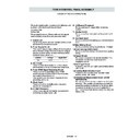
LSI(IX091DR)
The I/O signal of the LSI(IX091DR) are detailed in the following table.
The I/O signal of the LSI(IX091DR) are detailed in the following table.
Pin No.
Signal
I/O
Description
1-2
VL2-VL1
IN
Power source voltage input terminal.
Standard voltage for LCD.
Standard voltage for LCD.
3-5
AN7-AN5
IN
Terminal to change functions according to the Model.
DC voltage in accordance with the Model in operation is applied to set up its
function.
DC voltage in accordance with the Model in operation is applied to set up its
function.
6
AN4
IN
Temperature measurement input: OVEN THERMISTOR.
By inputting DC voltage corresponding to the temperature detected by the
thermistor, this input is converted into temperature by the A/D converter built
into the LSI.
By inputting DC voltage corresponding to the temperature detected by the
thermistor, this input is converted into temperature by the A/D converter built
into the LSI.
7
AN3
IN
Terminal not used.
8
AN2
IN
Input signal which communicates the door open/close information to LSI.
Door closed; "H" level signal.
Door opened; "L" level signal.
Door closed; "H" level signal.
Door opened; "L" level signal.
9-10
P61-P60
OUT
Timing signal output terminal for temperature measurement(OVEN
THERMISTOR)
"H" level (GND) : Thermistor OPEN timing.
"L" level (-5V) : Temperature measuring timing. (Convection cooking)
THERMISTOR)
"H" level (GND) : Thermistor OPEN timing.
"L" level (-5V) : Temperature measuring timing. (Convection cooking)
11
P57
IN
Terminal not used.
12
P56
OUT
Oven lamp and turntable motor driving signal(Square Waveform : 50Hz).
To turn on and off shut-off relay
(RY1). The square waveform voltage
is delivered to the relay (RY1) driving
circuit .
To turn on and off shut-off relay
(RY1). The square waveform voltage
is delivered to the relay (RY1) driving
circuit .
13
P55
OUT
Terminal not used.
14
P54
OUT
Signal to sound buzzer.
A: key touch sound.
B: Completion sound.
C: When the temperature of the oven
A: key touch sound.
B: Completion sound.
C: When the temperature of the oven
cavity reaches the preset temperature
in the preheating mode.
in the preheating mode.
D: When "SOUND ON" is set with the
SOUND key. When the MEMORY key
is continued to push for more than 5
seconds and the memory setting
condition is set.
is continued to push for more than 5
seconds and the memory setting
condition is set.
15
P53
OUT
Terminal not used.
16
P52
OUT
Fan motor driving signal.
To turn on and off the fan motor relay
RY5. "L" level during cooking, or for 90
seconds after manual cooking or 65
seconds after memory cooking (in case
where the same memory cooking is
operated for more than 10 minutes), or
until the oven cavity has been cooled
after convection or dual cooking.
To turn on and off the fan motor relay
RY5. "L" level during cooking, or for 90
seconds after manual cooking or 65
seconds after memory cooking (in case
where the same memory cooking is
operated for more than 10 minutes), or
until the oven cavity has been cooled
after convection or dual cooking.
17
P51
OUT
Bottom heater driving signal.
To turn on and off the bottom relay
(RY4). "L" level during grill (BOTTOM
HEATER, TOP AND BOTTOM) cooking
or dual (MICRO + BOTTOM) cooking or
convection cooking. "H" level otherwise.
To turn on and off the bottom relay
(RY4). "L" level during grill (BOTTOM
HEATER, TOP AND BOTTOM) cooking
or dual (MICRO + BOTTOM) cooking or
convection cooking. "H" level otherwise.
18
P50
OUT
Convection motor driving signal.
To turn on and off shut-off relay (RY7).
"L" level during CONVECTION; "H" level
otherwise.
To turn on and off shut-off relay (RY7).
"L" level during CONVECTION; "H" level
otherwise.
DESCRIPTION OF LSI
20 msec
During cooking
H
L
A
B
C
H: GND
L
0.12 sec
2.4 sec
1.2 sec
1.2 sec
D
0.08 sec
0.08 sec
0.08 sec
ON
OFF
During cooking, or for 90 sec.
after manual cooking or 65 sec.
after memory cooking, or until
the oven cavity has been cooled
after convection or dual cooking.
after manual cooking or 65 sec.
after memory cooking, or until
the oven cavity has been cooled
after convection or dual cooking.
H : GND
L : -5V
ON
OFF
During
cooking
L
GND
H.
(Convection)
ON
OFF
During
cooking
L
GND
H.
(Grill, dual or convection)
R-8740M - 24
Pin No.
Signal
I/O
Description
ON/OFF time ratio in Micro
cooking
(a. 32second time base)
(a. 32second time base)
ON/OFF time ratio in Micro
cooking
(a. 48second time base)
cooking
(a. 48second time base)
MICRO
ON
OFF
COOK
100%
100%
32sec.
0sec.
70%
24sec.
8sec.
50%
18sec.
14sec.
30%
12sec.
20sec.
10%
6sec.
26sec.
MICRO
ON
OFF
COOK
100%
100%
48sec.
0sec.
70%
36sec.
12sec.
50%
26sec.
22sec.
30%
16sec.
32sec.
10%
8sec.
40sec.
19
P47
OUT
Grill heater (TOP HEATER) driving signal.
To turn on and off the grill heater relay
(RY3). "L" level during grill (TOP
GRILL, TOP AND BOTTOM) cooking
or dual (MICRO + TOP) cooking or
convection cooking. "H" level
otherwise.
To turn on and off the grill heater relay
(RY3). "L" level during grill (TOP
GRILL, TOP AND BOTTOM) cooking
or dual (MICRO + TOP) cooking or
convection cooking. "H" level
otherwise.
20
P46
OUT
Magnetron high-voltage circuit driving signal.
To turn on and off the cook
relay (RY2). In 100%
POWER operation, the
signals hold "L" level during
microwave cooking and "H"
level while not cooking. In
other cooking modes (70%,
50%, 30%, 10%) the signal
turns to "H" level and "L"
level in repetition according
to the power level.
To turn on and off the cook
relay (RY2). In 100%
POWER operation, the
signals hold "L" level during
microwave cooking and "H"
level while not cooking. In
other cooking modes (70%,
50%, 30%, 10%) the signal
turns to "H" level and "L"
level in repetition according
to the power level.
21
P45
OUT
Memory (I-2) clock output.
22
P44
IN/OUT
Memory (I-2) data input/output.
23
INT1
OUT
Terminal not used.
24
INT0
IN
Signal to synchronized LSI with commercial power source
frequency(50Hz).
This is basic timing for time processing of LSI.
frequency(50Hz).
This is basic timing for time processing of LSI.
25
P41
IN
Terminal not used.
26
P40
IN
Connected to VC.
27
RESET
IN
Auto clear terminal.
Signal is input to reset the LSI to the initial state when power is applied.
Temporarily set to "L" level the moment power is applied, at this time the LSI
is reset. Thereafter set at "H" level.
Signal is input to reset the LSI to the initial state when power is applied.
Temporarily set to "L" level the moment power is applied, at this time the LSI
is reset. Thereafter set at "H" level.
28-29
P71-P70
OUT
Terminal not used.
30
XIN
IN
Internal clock oscillation frequency input setting.
The internal clock frequency is set by inserting the ceramic filter oscillation
circuit with respect to XIN terminal.
The internal clock frequency is set by inserting the ceramic filter oscillation
circuit with respect to XIN terminal.
31
XOUT
OUT
Internal clock oscillation frequency control output.
Output to control oscillation input of XOUT.
Output to control oscillation input of XOUT.
32
VSS
IN
Power source voltage: -5V.
VC voltage of power source circuit input.
VC voltage of power source circuit input.
33-36
P27-P24
OUT
Terminal not used.
37
P23
IN
Signal coming from touch key.
When any one of G4 line keys on key matrix is touched, a corresponding
signal from P17 - P12 will be input into P23. When no key is touched, the
signal is held at "H" level.
When any one of G4 line keys on key matrix is touched, a corresponding
signal from P17 - P12 will be input into P23. When no key is touched, the
signal is held at "H" level.
38
P22
IN
Signal similar to P23.
When any one of G3 line keys on key matrix is touched, a corresponding
signal will be input into P22.
When any one of G3 line keys on key matrix is touched, a corresponding
signal will be input into P22.
39
P21
IN
Signal similar to P23.
When any one of G2 line keys on key matrix is touched, a corresponding
signal will be input into P21.
When any one of G2 line keys on key matrix is touched, a corresponding
signal will be input into P21.
40
P20
IN
Signal similar to P23.
When any one of G1 line keys on key matrix is touched, a corresponding
signal will be input into P20.
When any one of G1 line keys on key matrix is touched, a corresponding
signal will be input into P20.
DESCRIPTION OF LSI
LSI(IX091DR)
The I/O signal of the LSI(IX091DR) are detailed in the following table.
The I/O signal of the LSI(IX091DR) are detailed in the following table.
ON
OFF
During
cooking
L
GND
H.
(Grill,dual or convection)
20 msec
H : GND
L (-5V)
R-8740M - 25
Pin No.
Signal
I/O
Description
41
P17
OUT
Key strobe signal.
Signal applied to touch-key section. A pulse signal is input to P20 - P23
terminal while one of G5 line keys on matrix is touched.
Signal applied to touch-key section. A pulse signal is input to P20 - P23
terminal while one of G5 line keys on matrix is touched.
42
P16
OUT
Key strobe signal.
Signal applied to touch-key section. A pulse signal is input to P20 - P23
terminal while one of G6 line keys on matrix is touched.
Signal applied to touch-key section. A pulse signal is input to P20 - P23
terminal while one of G6 line keys on matrix is touched.
43
P15
OUT
Key strobe signal.
Signal applied to touch-key section. A pulse signal is input to P207 - P23
terminal while one of G7 line keys on matrix is touched.
Signal applied to touch-key section. A pulse signal is input to P207 - P23
terminal while one of G7 line keys on matrix is touched.
44
P14
OUT
Key strobe signal.
Signal applied to touch-key section. A pulse signal is input to P20 - P23
terminal while one of G8 line keys on matrix is touched.
Signal applied to touch-key section. A pulse signal is input to P20 - P23
terminal while one of G8 line keys on matrix is touched.
45
P13
OUT
Key strobe signal.
Signal applied to touch-key section. A pulse signal is input to P20 - P23
terminal while one of G9 line keys on matrix is touched.
Signal applied to touch-key section. A pulse signal is input to P20 - P23
terminal while one of G9 line keys on matrix is touched.
46
P12
OUT
Key strobe signal.
Signal applied to touch-key section. A pulse signal is input to P20 - P23
terminal while one of G10 line keys on matrix is touched.
Signal applied to touch-key section. A pulse signal is input to P20 - P23
terminal while one of G10 line keys on matrix is touched.
47-48
P11-P10
IN
Terminal not used.
49
P07
OUT
Cooking mode indicator driving signal.
To turn on and off the light emitting diode LD9.
To turn on and off the light emitting diode LD9.
50
P06
OUT
Cooking mode indicator driving signal.
To turn on and off the light emitting diode LD8.
To turn on and off the light emitting diode LD8.
51
P05
OUT
Cooking mode indicator driving signal.
To turn on and off the light emitting diode LD6.
To turn on and off the light emitting diode LD6.
52
P04
OUT
Cooking mode indicator driving signal.
To turn on and off the light emitting diode LD7.
To turn on and off the light emitting diode LD7.
53-56
P03-P00
OUT
Terminal not used.
57-60
P37-P34
OUT
Terminal not used.
61-72
SEG11-SEG0
OUT
Segment data signal.
Connected to LCD.
The relation between signals are as follows:
Connected to LCD.
The relation between signals are as follows:
LSI signal (Pin No.)
LCD (Pin No.)
LSI signal (Pin No.) LCD (Pin No.)
SEG 0 (72) .............................. S1
SEG 6 (66) ............................ S7
SEG 1 (71) .............................. S2
SEG 7 (65) ............................ S8
SEG 2 (70) .............................. S3
SEG 8 (64) ............................ S9
SEG 3 (69) .............................. S4
SEG 9 (63) .......................... S10
SEG 4 (68) .............................. S5
SEG10 (62) ......................... S11
SEG 5 (67) .............................. S6
SEG11 (61) ......................... S12
73/74
VCC/VREF
IN/IN
Connected to GND.
75
AVSS
IN
Connected to VC.
76
COM3
OUT
Terminal not used.
77
COM2
OUT
Common data signal: COM3.
Connected to LCD (Pin No. 3).
Connected to LCD (Pin No. 3).
78
COM1
OUT
Common data signal: COM2.
Connected to LCD (Pin No. 2).
Connected to LCD (Pin No. 2).
79
COM0
OUT
Common data signal: COM1.
Connected to LCD (Pin No. 1).
Connected to LCD (Pin No. 1).
80
VL3
IN
Power source voltage input terminal.
Standard voltage for LCD.
Standard voltage for LCD.
DESCRIPTION OF LSI
LSI(IX091DR)
The I/O signal of the LSI(IX091DR) are detailed in the following table.
The I/O signal of the LSI(IX091DR) are detailed in the following table.
R-8740M - 26
I-2 is a 2K-bit, serial memory, enabling CMOS to be erased/written electrically. This memory is constructed with
256 registers x 8bits, enabling individual access, read and write operations to be performed. Details of input/
output signal for I-2 are as shown in the following diagram.
256 registers x 8bits, enabling individual access, read and write operations to be performed. Details of input/
output signal for I-2 are as shown in the following diagram.
Table 2. Relation between Pin Nos, and Signals
Pin No.
Signal
I/O
Description
1-3
A0-A2
IN
Connected to +5V.
4
VSS
IN
Connected to GND.
5
SDA
IN/OUT
Serial data input/output : input/outputs data to I-1.
6
SCL
IN
Clock signal input : input/outputs serial data at every one pulse.
7
TEST
IN
Connected to GND.
8
VCC
IN
Connected to +5V.
Memory IC (I-2)
Display

