Sharp DV-740 (serv.man13) Service Manual ▷ View online
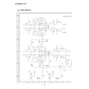
78
DV-740H/S(Y,F,S,R)
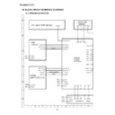
79
DV-740H/S(Y,F,S,R)
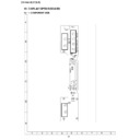
80
DV-740H/S(Y,F,S,R)
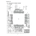
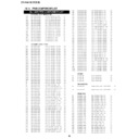
Data Bus
Data Bus
Port 0
Drivers
P0.7:0
Port 2
Drivers
P2.7:0
Data Bus
Data Bus
Program Address
Register
Program Counter
Buffer
DPTR
Incrementer
Port 1
Drivers
P1.7:0
Port 3
Drivers
P3.7:0
Port Latch
Port Latch
Port Latch
Serial Port
Timer
Interrupt Logic
ACC
ALU REG1
ALU REG2
PSW
ALU
B Register
Stack
Pointer
Clocks and Control
OSC
Instruction
Register
RAM Addr.
Register
512 Bytes
RAM
XTAL1
XTAL2
/PSEN
ALE
/EAVPP
RST
64K bytes
MTP Memory
81
DV-740H/S(Y,F,S,R)
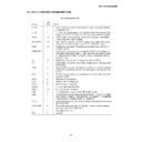
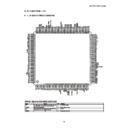
Pin Name No. (PLCC) Type
Description
VDD
44
IN
Power supply for internal operation, 5V input.
GND
22
IN
Ground.
P0.7-P0.0
36,37,38,39,
40,41,42, 43
40,41,42, 43
I/O
Port 0 is 8 bits bi-directional I/O port with internal pull high.
AD7-0
Multiplexed address/data bus. During the time when ALE is high, the LSB of a
memory address is presented. When ALE falls, the port transitions to a
bi-directional data bus. This bus is used to read external ROM and read/write
external RAM memory or peripherals.
memory address is presented. When ALE falls, the port transitions to a
bi-directional data bus. This bus is used to read external ROM and read/write
external RAM memory or peripherals.
RST
10
IN
Reset signal of internal circuit, it must be kept 4 clocks to ensure being recognized
by internal circuit. This signal will not affect internal SRAM.
by internal circuit. This signal will not affect internal SRAM.
XTAL1
21
IN
Crystal In , can be used as external clock input.
XTAL2
20
OUT
Crystal out, feedback of XTAL1.
/PSEN
32
OUT
Program Store Enable Output, commonly connected to external ROM memory as a
chip enable during fetching and MOVC operation. /PSEN goes high during a reset
condition.
chip enable during fetching and MOVC operation. /PSEN goes high during a reset
condition.
ALE
33
OUT
Address Latch Enable, used to latch external LSB 8 bit address bus from
multiplexed address/data bus, commonly connect to the latch enable of 373
families. This signal will be forced high when the device is in a reset condition.
multiplexed address/data bus, commonly connect to the latch enable of 373
families. This signal will be forced high when the device is in a reset condition.
P1.7-P1.0
9,8,7,6,5,4,3
,2
,2
I/O
Port 1 is 8 bits bi-directional I/O port with internal pull high. All pins have an alternate
function shown as below.
function shown as below.
T2EX (P1.1)
IN
External timer/counter 2 trigger.
T2 (P1.0)
IN
External timer/counter 2.
P2.7-P2.0
31,30,29,28,
27,26,25, 24
27,26,25, 24
I/O
Port 2 is 8 bits bi-directional I/O port with internal pull high. The alternate function is
MSB 8 bit address bus
MSB 8 bit address bus
A15-A8
OUT
This bus emits the high-order address byte during fetches from external Program
Memory or during accesses to external Data Memory that use 16-bit addresses
(MOVX @ DPTR).
During accesses to external Data Memory that use 8-bit addresses (MOVX @ Ri),
Port 2 emits the contents of the P2 Special Function Register.
Memory or during accesses to external Data Memory that use 16-bit addresses
(MOVX @ DPTR).
During accesses to external Data Memory that use 8-bit addresses (MOVX @ Ri),
Port 2 emits the contents of the P2 Special Function Register.
P3.7-P3.0
19,18,17,16,
15,14,13, 11
15,14,13, 11
I/O
Port 3 is an 8-bit bi-directional I/O port with internal pull high. The reset condition of
this port is with all bits at a logic 1.
Port 3 also have alternate function list below
this port is with all bits at a logic 1.
Port 3 also have alternate function list below
/RD (P3.7)
OUT
External data memory read strobe.
/WR (P3.6)
OUT
External data memory writes strobe.
T1 (P3.5)
IN
External timer/counter 1.
T0 (P3.4)
IN
External timer/counter 0.
/INT1 (P3.3)
IN
External interrupt 1 (Negative Edge Detect).
/INT0 (P3.2)
IN
External interrupt 0 (Negative Edge Detect).
TXD (P3.1)
OUT
Serial port output.
RXD (P3.0)
IN
Serial port input.
/EAVPP
35
IN
The pin must be externally held low to enable the device to fetch code from external
program memory. If /EAVPP is held high, the device executes from internal
program memory. /EAVPP is internal latched on reset. This pin also receives the
12V programming voltage (V
program memory. If /EAVPP is held high, the device executes from internal
program memory. /EAVPP is internal latched on reset. This pin also receives the
12V programming voltage (V
PP
) during FLASH programming.
NC
1,12,23,34 NC
These pins should not be connected for any purpose


