Sharp XL-S10H (serv.man8) Service Manual ▷ View online
XL-S10H
6 – 1
Audio
XL-S10H
Service Manual
XS10H
Market
E
CHAPTER 6.
CIRCUIT SCHEMATICS AND PARTS LAYOUT
[1] NOTES ON SCHEMATIC DIAGRAM
•
Resistor:
To differentiate the units of resistors, such symbol as K and M are
used: the symbol K means 1000 ohm and the symbol M means
1000 kohm and the resistor without any symbol is ohm-type resis-
tor. Besides, the one with “Fusible” is a fuse type.
used: the symbol K means 1000 ohm and the symbol M means
1000 kohm and the resistor without any symbol is ohm-type resis-
tor. Besides, the one with “Fusible” is a fuse type.
•
Capacitor:
To indicate the unit of capacitor, a symbol P is used: this symbol P
means micro-micro-farad and the unit of the capacitor without such
a symbol is microfarad. As to electrolytic capacitor, the expression
“capacitance/withstand voltage” is used.
means micro-micro-farad and the unit of the capacitor without such
a symbol is microfarad. As to electrolytic capacitor, the expression
“capacitance/withstand voltage” is used.
(CH), (TH), (RH), (UJ): Temperature compensation
(ML): Mylar type
(P.P.): Polypropylene type
•
Schematic diagram and Wiring Side of P.W.Board for this model
are subject to change for improvement without prior notice.
are subject to change for improvement without prior notice.
•
The indicated voltage in each section is the one measured by Digi-
tal Multimeter between such a section and the chassis with no sig-
nal given.
tal Multimeter between such a section and the chassis with no sig-
nal given.
1. In the tuner section,
( ) indicates AM
< > indicates FM stereo
2. In the main section, a tape is being played back.
3. In the deck section, a tape is being played back.
( ) indicates the record state.
4. In the power section, a tape is being played back.
5. In the CD section, the CD is stopped.
•
Parts marked with “
” (
) are important for
maintaining the safety of the set. Be sure to replace these parts
with specified ones for maintaining the safety and performance of
the set.
with specified ones for maintaining the safety and performance of
the set.
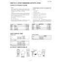
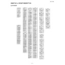
[2] IC701 SERIAL No. TABLE
IXA006SJ - FLASH
IXA007SJ - 1st MASK
IXA019SJ - 2nd MASK
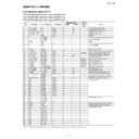
[3] TYPES OF TRANSISTOR AND LED
REF. NO
DESCRIPTION
POSITION
SW501
PLAY
ON—OFF
SW700
VOLUME
ON—OFF
SW701
CD LID
ON—OFF
SW702
ON/STAND-BY
ON—OFF
SW703
FUNCTION
ON—OFF
SW704
BASS/TRBLE
ON—OFF
SW705
MEMORY/SET
ON—OFF
SW707
TUNING UP
ON—OFF
SW708
TUNING DOWN
ON—OFF
SW709
PRESET UP
ON—OFF
SW710
PRESET DOWN
ON—OFF
SW711
CLEAR
ON—OFF
REF. NO
DESCRIPTION
POSITION
Serial No.
Europe
No.31000001~ 31208729
No.31227730 ~ 31234729
No.31227730 ~ 31234729
U.K.
No. 31000001 ~ 31204002
Serial No.
Europe
No.31108730~ 31227729
No.40134730 ~ 40148929
No.40150930 ~ 40151429
No.40134730 ~ 40148929
No.40150930 ~ 40151429
U.K.
No. 40104003 ~ 40105002
Australia/New Zealand
No.31202006 ~ 31202505
Serial No.
Europe
No.40148930 ~ 40150929
No.40251430 ~
No.40251430 ~
U.K.
No.40205003 ~
Australia/New Zealand
No.40202506 ~
(1) (2) (3)
(S) (G) (D)
E C B
FRONT
VIEW
FRONT
VIEW
2SC5395 F+
SVC201
FRONT
VIEW
B C E
FRONT
VIEW
2SB1370 E+
2SC3052 F+
2SC5477++
2SA1235 F+
B
E
C
SVC347S
MPG3372X
XL-S10H
6 – 2
[4] WIRING SIDE OF P.W.BOARD/SCHEMATIC DIAGRAM
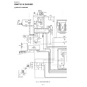
Figure 6-2 SCHEMATIC DIAGRAM (1/8)
A
B
C
D
E
F
G
H
1
2
3
4
5
6
6-4,6-5 2~11 - A
SVC201
SVC201
4.7/50
75kHz
100K
10P(CH)
0.1
47K
1K
390
10µH
47µH
1/50
1/50
0.01
1
2
3
2
3
1µH
1/50
AM ANT.
BAND PASS
FILTER
FILTER
10
0.001
10P
0.1
33
100
330
2.2K
680
2SC5477++
1SS133
1SS133
0
0
2 3
4
5
6
7
1
0
22/50
1/50
0.001
5P(CH)
0.1
0.001
100P
FM
IF
FM IF
FM IF
AM IF
AM IF
33P
33P
(UJ)
(UJ)
(UJ)
5P
0.01
0.01
0.001
100K
2SC5477++
220
100K
2.2K
1K
4.7K
22/50
0.1
1K
0.01
0.1
330
0.022
22/50
4.7K
0.01
0.1
+B
+B
+B
+B
+B
+B
+B
+B
+B
+B
+B
+B
+B
+B
+B
+B
+B
0.1
0.47/50
0
47
10K
22/50
10K
MTZJ3.6B
1K
1K
47K
1K
100K
MTZJ120B
10P(CH)
2SC3052F+
0.33/50
100P(CH)
100K
100K
20P
(CH)
0.01
1
2
3
2
3
100P
100P
3.3K
1/50
10µH
10
0.1
0.1
3
2
1
6
5
4
3
2
1
4
5
6
100K
SVC347S
19
20
21
36
35
34
1
2
3
18
17
16
4
5
6
7
8
9
10
11
12
13
14
15
LV23002M
33
32
31
560P
27P
(CH)
3
2
1
6
5
4
0.022
22
23
24
25
26
27
28
29
30
VP
VTCC
FM:1.5V-5.0V
AM:1V-8V
TP-VT
FMRF-IN
FMRF-OUT
VCC2
FM-OSC
AM-OSC
B02
B01
LP-OUT
LP-IN
PD
AGC
AMLOWOUT
DET-OUT
MPX-IN
VDD
XOUT
XIN
D0
CL
DI
R-OUT
L-OUT
FM-IET
P-CCMP
P-DET
CE
VSS
P-DET
FMRF-IN
VCC1
AM-MIX
GND1
FM-MIX
REG
AMRF-IN
AM LOOP
ANTENNA
FM ANTENNA
TO MAIN PWB
AMP./TAPE SEC
MAIN PWB-A1(1/2)
FM
RF
FM
OSC.
FM
BAND
COVERAGE
fL
FM
FRONT
END
NOTES ON SCHEMATIC DIAGRAM can be found on page 6-1
CNP301
C301
D302
D303
JR304
L302
D307
D306
C309
C307
L304
JR302
C317
C316
C318
C314
L307
R328
R307
R305
C306
C308
R303
C305
R304
D305
C311
C310
C345
R310
L306
R311
C332
C329
C335
C321
R327
C344
R314
C343
C333
R316
C312
R308
R329
C320
R313
D308
C325
X301
R319
C341
C342
C351
R315
C326
C330
C338
R326
R324
R322
D309
Q301
L308
C340
R325
R318
R317
C328
C324
C327
C322
C331
C323
CF303
L305
C372
R371
R374
R375
R376
Q371
CF304
JR303
R372
C315
C313
R312
C319
R309
CF302
C334
C337
C336
R321
R320
C339
R323
L303
R302
C302
C303
L301
IC301
C801
R306
L801
CF301
CF306
Q302
PLL(TUNER)
FM
IF
DET./FM
M
PX./AM
IF
AM BAND
COVERAGE fL
COVERAGE fL
AM
Tracking
Tracking
XL-S10H
6 – 3
Figure 6-3 SCHEMATIC DIAGRAM (2/8)
7
8
9
10
11
12
IC701:
IXA007SJ
6-6
2
-
D
IC701:
IXA006SJ/IXA019SJ
6-8
2
-
D
CNS701
6-4,6-5 2~11 - A
33K
33K
0
µH
100K
8 9 10
11 12 13
14 15 16 17
MTZJ3.9B
6.8K
6.8K
MTZJ5.1B
6.8K
6.8K
6.8K
10
18
13
14
12
11
15
17
16
1
2
3
4
5
6
7
8
9
6.8K
6.8K
6.8K
6.8K
0.1
100P
47K
15K
B
B
+B
+B
+B
+B
+B
+B
+B
+B
+B
+B
+B
+B
+B
+B
1/50
1/50
18
+B
18
18
0.1
100
100
0.1
0.1
15K
10K
1K
12
12
2SC3052F+
2SC5395F+
100
12K
10K
6.8K
1K
0.1
100/10
330
100
470
1K
0.1
12P(CH)
12P(CH)
16.9344MHz
10K
100P(CH)
100P(CH)
0.1
33/16
33K
100K
33K
0.1
100/6.3
100/6.3
100/6.3
0.1
470
10
2SA1235F+
12K
0.1
0.047
1/50
100K
0.047
0.1
100P
330
0.0022
10K
10/16
47P
0.0022
10/16
47
100/6.3
0.1
0.1
0.1
680
680
1.2K
27K
220
1
2
3
20 19 18
21
22
22
3
2
38
39
40
39
40
4142 43
585960
61
62
63
80
79
78
79
78
LA6548D
13
14
15
16
12 11 10
1
2
3
4
5
6
7
8
9
1 2 3 4 5 6 7
1 2 3 4 5 6
LC78646E
4
5
6
7
8
9
10
11
12
13
14
15
16
17
24
25
25
6
2
27
28
27
28
9
2
30
31
32
33
34
30
31
32
33
34
5
3
36
36
7
3
4445 6
4 47 4849 0
5 5152 535455 6
5 57
64
65
66
67
68
69
70
71
72
73
74
75
76
77
VP
D-GND
0-POWER
1-TP-STATE
0-EVRCLK
0-EVR-SD0
0-AMP-ON
0-TU-CE
0-TU-SDO
0-TU-SCK
1-TU-SDI
0-CD-CE
I-CD-WRQ
0-CD-CLK
O-CD-CMD
1-CD-DATA
0-CD-/RESET
I-CD-DRF
FE
RFMON
TP7
TP6
TP5
1-SLD
G-SLD
0+SLD
0-SLD
TCAP
RESET
RESET
REG-TR
0-SPD
0+SPD
G-SPD
REF-IN
1-SPD
1-SPD
G-TRK
REG-OUT
0+TRK
0-TRK
0-FCS
I-TRK
G-FCS
1-FCS
GND
GND
GND
GND
0+FCS
GND
GND
GND
GND
GND
MUTE
VCCVCC
VWRQ
VRES
DRF
CE
CL
DI
DO
CONT3
CONT2
PD01
PD02
VVSS
PCKIST
VVDD
VDD5
VSS
LDD
FR
LDS
DATA
DATACK
REF1
TDO
ADAVSS
ADAVDD
JITTC
RFMON
TE
TEC
FE
RSVSS
RFVDD
RF
VREF
TIN2F
TIN1E
FIN2B
FIN1A
LCHO
LVSS
RVSS
RCHO
RVDD
XVDD
EFMIN
SLCIST
SLCO
XOUT
XIN
FSX/16MIN
XVSS
C2F
EFLG
IGMOUT
ASRACK
ASDFIN
LRSY
TEST
DOUT
VDD
VSS
MON15
MON14
MON13
ASDACK
MON12
DEFECT
SBCK/FG
CONT5
CONT4
GPDAC
SLDO
SPDO
MON11
FSEQ
V/1P
FDO
30
29
28
27
26
25
24
23
22
21
20
19
18
17
16
29
28
27
26
25
24
23
22
21
20
19
18
17
16
15
14
13
12
11
10
9
8
7
6
5
4
3
2
1
F
B
A
E
+
+
+
+
+
-
-
-
-
-
FO+
TR+
TR-
FO-
ACTUATOR
TR+
FO+
FO-
C
F
B
A
E
1/2V
+5V
TR-
1/2VCC
C
-
+
D
VCC
VC
LD
VR
MD
D
GND
GND
LD
VR
MD(PD)
CD PICKUP UNIT
CD MECHANISM UNIT (227)
MECHANISM PWB
+
+
–
–
SP+
SP–
SL+
SL–
PU-IN
GND
PICKUP IN
SLED
MOTOR
SPINDLE
MOTOR
M
M
5
1
4
6
2 3
16 15 14 13 12 11 10
9
8
7
6
5
4
3
2
1
CD SERVO
FOCUS/TRACKING/
SPIN/SLED DRIVER
SPIN/SLED DRIVER
FROM
DISPLAY
P
WB
TO MAIN PWB (2/2)
AMP./TAPE SECTION
LVDD
TP8
IC802
C803
R812
C802
C801
CNW802
CNS802
CNS801
CFW801
R814
R816
R813
R815
R821
Q803
C814
C815
R826
R824
R822
R830
JR801
R832
R829
R827
R828
C820
R831
D801
C826
C825
C829
C824
C827
R833
C832
C831
C830
R836
C828
C817
C813
R834
C823
C816
C811
C819
C808
C807
R817
R818
C818
C821
R823
C810
C809
C812
R825
X801
R551
R559
R558
R552
R553
R555
R556
R557
R554
C833
C834
R841
CNP503
R546
R545
R544
C838
R842
C837
C836
C835
R839
R840
R838
IC801
C806
R809
R811
R810
R808
D802
C804
R806
R803
R801
R804
R802
Q801
Q802
801
R837
FM SIGNAL
AM SIGNAL
CD SIGNAL
XL-S10H
6 – 4
Figure 6-4 SCHEMATIC DIAGRAM (3/8)
A
B
C
D
E
F
G
H
1
2
3
4
5
6
6-2,6-3 2~11 - H
3.3K
0.0022
6.8K
1/50
6.8K
1
3
2
4
1
2
3
2
3
0.0022
100
2SB1370E+
2.2K
47/25
1K
1K
10
10
220/6.3
0.1
1K
8.2K
8.2K
1/50
4.7K
4.7K
NOT USED
0.1
1.5K
100/16
0.0022
33K
3.3K
3.3K
22/50
220
220
0.1
10
10
0.1
0.1
0.1
0.1
10
0.1
0.1
0.1
1000/16
1/50
22/50
4.7/50
330K
0.1
0.1
22K
0.047
1µH
0.1
0.1/50
6.8K
1/50
4.7K
680
220/16
0.01
2SC3052F+
1SS133
6800/25
0.1
0.1
1N4004A
1N4004A
1N4004A
2SC3052F+
0.0022
MTZJ6.8B
0.1
1N4004A
100
33K
1000/16
47/25
+B
+B
+B
+B
+B
+B
+B
+B
+B
+B
+B
+B
+B
+B
+B
+B
+B
+B
+B
+B
+B
+B
2SC5395F+
330K
22K
10P
1
2
3
4
5
7
6
12
10
9
8
11
13
15
6
1
(CH)
13
14
LA4631++
POWER AMP.
+
–
–
+
10
AMP_A1_ON
(R)
(L)
CD_A1_P_A1_GND
CD_A1_VCC
EMC-GND
EMC-GND
TP-GND
D-GND
A-GND
SP-GND
P-ON
TP-VM
MA-VCC
GND
SD
OUT2
BB2
1 2 3
POWER
TRANSFORMER
T315mA L 250V
POWER PWB-A3
When Servicing,
Pay attention as the area enclosed
by this line (
Pay attention as the area enclosed
by this line (
) is directly
connected with AC main voltage.
AC POWER
SUPPLY CORD
AC 230 V, 50 Hz
HEADPHOMES
SPEAKER
TERMINAL
L-CH
R-CH
2 3
4
5
6
7
1
TO MAIN PWB (1/2)
TUNER/CD SECTION
MAIN PWB-A1(2/2)
S101
NOT USED
2
1
L
R
J102
J104
NOTES ON SCHEMATIC DIAGRAM can be found on page 6-1
C112
C130
R119
R120
R121
C111
R105
R108
C110
IC101
C116
C120
C115
C122
C123
C121
C125
R131
C133
C119
R117
R116
R112
C127
R113
C126
C117
C134
R132
L103
C105
R106
R103
C109
C104 C108
L102
C102
R104
C106
C107
C103
R107
J101
R102
R101
J103
L101
C101
F653
CNP101
CNW101
CNS101
D104
C113
C114
D101
D103
D102
Q101
R118
R110
R111
C129
C124
Q103
D106
C118
Q102
D105
C128
R109
R114
R502
C505
R549
R550
R503
R501
C502
C501
Q502
C506
R507
C504
C503
R505
R504
R508
C507
R509
C508
PT1
R115

