Sharp XL-MP35H (serv.man20) Service Manual ▷ View online
XL-MP35H
– 34 –
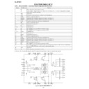
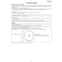
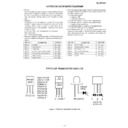
FUNCTION TABLE OF IC
IC401 VHiLC75342M-1: Function/Volume Equaliser (LC75342M)
1
DI
Serial data and clock input pin for control.
2
CE
Chip enable pin. Data written into an internal latch in a timing of [H] -> [L]. Each analog switch is activated.
Data transfer enabled at [H] level.
Data transfer enabled at [H] level.
3
VSS
Ground pin.
4
TEST
Electronic volume control pin. To be set to the VSS potential.
5
LOUT
Volume + equalizer output pin.
6
LBASS2
Bass-band filter comprising capacitor and resistor connection pin.
7
LBASS1
Bass-band filter comprising capacitor and resistor connection pin.
8
LTRE
Capacitor connection pin comprising treble band filter.
9
LIN
Volume + equalizer input pin.
10
LSEL0
Input selector output pin.
11
L4
Input signal pin.
12-14
L3-L1
Input signal pin.
15*
NC
No CONNECT pin. To be open or connected to VSS.
16*
NC
No CONNECT pin. To be open or connected to VSS.
17-19
R1-R3
Input signal pin.
20
R4
Input signal pin.
21
RSEL0
Input selector output pin.
22
RIN
Volume + equalizer input pin.
23
RTRE
Capacitor connection pin comprising treble band filter.
24
RBASS1
Bass-band filter comprising capacitor and resistor connection pin.
25
RBASS2
Bass-band filter comprising capacitor and resistor connection pin.
26
ROUT
Volume + equalizer output pin.
27*
NC
No CONNECT pin. To be open or connected to VSS.
28
Vref
0.5 x VDD voltage generation block for analog ground. Capacitor of several 10
µ
F to be connected between
Vref and AWSS (VSS) as a counter measure against power ripple.
29
VDD
Supply pin.
30
CL
Serial data and clock input pin for control.
Pin No.
Port Name
Function
In this unit, the terminal with asterisk mark (*) is (open) terminal which is not connected to the outside.
6
7
8
9
10
11
12
13
14
15
16
17
18
19
20
21
22
23
24
25
26
5
27
28
30
29
1
2
3
4
LVref
RVref
CCB
INTERFACE
CONTROL
CIRCUIT
LOGIC
CIRCUIT
CONTROL
CIRCUIT
ROUT
RBASS1
RBASS2
RTRE
RIN RSEL0
L1
L2
L3
L4
R1
R2
R3
R4
LOUT
LBASS2 LBASS1
LTRE
LIN
LSEL0
VSS
CE
DI
CL
VDD
NC
Vref
NC
NC
TEST
Figure 34 BLOCK DIAGRAM OF IC
– 35 –
XL-MP35H
14,55,89 VSS1,VSS2,
—
Power supply positive terminal
VSS3
17,54,90 VDD1,VDD2
—
Power supply negative terminal
VDD3
1,2
PORT0
Input/Output
• 8-bit I/O port • Specifiable 4 bit by 4 bit • Pull-up resistor can be ON/OFF 4 bit by 4 bit
95~100
P00~P07
• HOLD release input
• Port 0 interrupt input
3~10
PORT1
Input/Output
• 8-bit I/O port
P10~P17
• Specifiable bit by bit
• Pull-up resistor can be ON/OFF 1bit by 1bit
• Usable as
P10: SIO0 data output P11: SIO0 data input & bus input/output
P12: SIO0 clock input/output
• Pull-up resistor can be ON/OFF 1bit by 1bit
• Usable as
P10: SIO0 data output P11: SIO0 data input & bus input/output
P12: SIO0 clock input/output
P13: SIO1 data output
P14: SIO1 data input & bus input/output
P15: SIO1 clock input/output
P15: SIO1 clock input/output
P16: Timer 1PWML output
P17: Timer 1PWMH output/buzzer output
87*,88*
PORT3
Input/Output
• 6 -bit I/O port
32~35
P30~P35
• Specifiable 1bit by 1bit
• Pull-up resistor can be ON/OFF 1bit by 1bit
• Usable as
P30 - P33:INT4 input/HOLD release input/Timer 1 event input/Timer 0L capture input/Timer
0H capture input
P34 & P35:INT5 input/HOLD release input/Timer 1 event input/Timer 0L capture input/Timer
0H capture input
• Interrupt system
• Pull-up resistor can be ON/OFF 1bit by 1bit
• Usable as
P30 - P33:INT4 input/HOLD release input/Timer 1 event input/Timer 0L capture input/Timer
0H capture input
P34 & P35:INT5 input/HOLD release input/Timer 1 event input/Timer 0L capture input/Timer
0H capture input
• Interrupt system
26,27*
PORT7
Input/Output
• 4-bit I/O port
28,29
P70~P73
• Specifiable 1bit by 1bit
• Pull-up resistor can be ON/OFF 1bit by 1bit
• Usable as
P70:INT0 input/Hold release input/Timer 0L capture input/Watchdog timer output
P71:INT1 input/Hold release input/Timer 0H capture input
P72:INT2 input/Hold release input/Timer 0 event input/Timer 0L capture input
P73:INT3 input (with noise filter)/Timer 0 event input/Timer 0H capture input
A/D conversion input port: AN8 (P70), AN9 (P71)
• Interrupt system
22*,25*
PORT8
Input/Output
• 8-bit I/O port
18~21
P80~P87
• 1-bit oriented input/output
23,24
• Usable as
A/D conversion input port: AN0 - AN7
Small signal detect input port: MICIN (P87)
A/D conversion input port: AN0 - AN7
Small signal detect input port: MICIN (P87)
Pin No.
Function
PORT Name
Input/Output
In this unit, the terminal with asterisk mark (*) is (open) terminal which is not connected to the outside.
IC701 RH-iX0073SJZZ: System Microcomputer (IX0073SJ) (1/2)
INT0
INT1
INT2
INT3
INT1
INT2
INT3
Rise
Fall
Rise & Fall
H level
L level
INT0
INT1
INT2
INT3
INT1
INT2
INT3
Rise
Fall
Rise & Fall
H level
L level
XL-MP35H
– 36 –
Function
Terminal Name Input/Output
30~37
S0/PA0~S7/PA7 Input/Output
• LCD segment output
• Usable as general purpose I/O port (PA)
• Usable as general purpose I/O port (PA)
38~40,41* S8/PB0~
Input/Output
• LCD segment output
42~45
S15/PB7
• Usable as general purpose I/O port (PB)
46~53
S16/PC0~
Input/Output
• LCD segment output
S23/PC7
• Usable as general purpose I/O port (PC)
56~63
S24/PD0~
Input/Output
• LCD segment output
S31/PD7
• Usable as general purpose I/O port (PD)
64~71
S32/PE0~
Input/Output
• LCD segment output
S39/PE7
• Usable as general purpose I/O port (PE)
72~79
S40/PF0~
Input/Output
• LCD segment output
S47/PF7
• Usable as general purpose I/O port (PF)
83~86
COM0/PL0~
Input/Output
• LCD common output
COM3/PL3
• Usable as general purpose input port (PL)
80~82
V1/PL4~
Input/Output
• LCD drive bias voltage
V3/PL6
• Usable as general purpose input port (PL)
• Usable as
A/D conversion input port: AN12 - AN14
• Usable as
A/D conversion input port: AN12 - AN14
11
RES
Input
Reset terminal
12
XT1
Input
• 32.768 kHz crystal oscillator input terminal
• Usable as
• General purpose input port
• Connect to VDD1 when not in use.
A/D conversion input port: AN10
• Usable as
• General purpose input port
• Connect to VDD1 when not in use.
A/D conversion input port: AN10
13
XT2
Input/Output
• 32.768 kHz crystal oscillator output terminal
• Usable as
General purpose input port
Set as oscillator and leave open when not in use.
A/D conversion input port: AN11
• Usable as
General purpose input port
Set as oscillator and leave open when not in use.
A/D conversion input port: AN11
15
CF1
Input
• Ceramic oscillator input terminal
16
CF2
Output
• Ceramic oscillator output terminal
Pin No.
IC701 RH-iX0073SJZZ: System Microcomputer (IX0073SJ) (2/2)
P06
P07
P10/SO0
P11/SI0/SB0
P12/SCK0
P13/SO1
P14/SI1/SB1
P15/SCK1
P16/T1PWML
P17/T1PWMH/BUZ
RES
XT1/AN10
XT2/AN11
VSS1
CF1
CF2
VDD1
P80/AN0
P81/AN1
P82/AN2
P83/AN3
P84/AN4
P85/AN5
P86/AN6
P87/AN7/MICIN
P70/INT0/T0LCP/AN8
P71/INT1/T0HCP/AN9
P72/INT2/T0IN
P73/INT3/T0IN
S0/PA0
S1/PA1
S2/PA2
S3/PA3
S4/PA4
S5/PA5
S6/PA6
S7/PA7
S8/PB0
S9/PB1
S10/PB2
S11/PB3
S12/PB4
S13/PB5
S14/PB6
S15/PB7
S16/PC0
S17/PC1
S18/PC2
S19/PC3
S20/PC4
S21/PC5
S22/PC6
S23/PC7
S24/PD0
S25/PD1
S26/PD2
S27/PD3
S28/PD4
S29/PD5
S30/PD6
S31/PD7
S32/PE0
S33/PE1
S34/PE2
S35/PE3
S36/PE4
S37/PE5
S38/PE6
S39/PE7
S40/PF0
S41/PF1
S42/PF2
S43/PF3
S44/PF4
S45/PF5
S46/PF6
S47/PF7
V3/PL6/AN14
VDD2
VSS2
80
79
78
77
76
75
74
73
72
71
70
69
68
67
66
65
64
63
62
61
60
59
58
57
56
55
54
53
52
51
1
2
3
4
5
6
7
8
9
10
11
12
13
14
15
16
17
18
19
20
21
22
23
24
25
26
27
28
29
30
V2/PL5/AN13
V1/PL4/AN12
COM0/PL0
COM1/PL1
COM2/PL2
COM3/PL3
P30/INT4/T1IN
P31/INT4/T1IN
VSS3
VDD3
P32/INT4/T1IN
P33/INT4/T1IN
P34/INT5/T1IN
P35/INT5/T1IN
P00
P01
P02
P03
P04
P05
81
82
83
84
85
86
87
88
89
90
91
92
93
94
95
96
97
98
99
100
50
49
48
47
46
45
44
43
42
41
40
39
38
37
36
35
34
33
32
31
Figure 36 BLOCK DIAGRAM OF IC
In this unit, the terminal with asterisk mark (*) is (open) terminal which is not connected to the outside.
– 37 –
XL-MP35H
IC801 VHiLC78646E-1: Servo/Signal Control (LC78646E) (1/2)
1
SLCO
Output
—
Control output.
2
SLCIST
Input
—
Resistor connection terminal for SLCO output current setting.
3
EFMIN
Input
—
RF signal input terminal.
4
RF
Output
—
RF signal monitor terminal.
5
RFVDD
Input
—
RF power terminal.
6
RFVSS
—
—
RF earth terminal. To be connected to 0 V.
7
FIN1
Input
—
A+C signal input terminal.
8
FIN2
Input
—
B+D signal input terminal.
9
TIN1
Input
—
E signal input terminal.
10
TIN2
Input
—
F signal input terminal.
11
VREF
Output
RFVDD/2
VREF voltage output terminal.
12
REF1
Input
—
Reference supply setting terminal.
13*
FE
Output
ZHI
FE signal monitor terminal.
14
TEC
Output
—
LPF capacitor connection terminal for TE signal.
15
TE
Output
ZHI
TE signal monitor terminal.
16*
RFMON
Output
ZHI
RF internal signal monitor terminal.
17
JITTC
—
—
Capacitor connection terminal for jitter detection.
18
ADAVDD
Input
—
Power terminal for servo A/D, D/A.
19
ADAVSS
—
—
Earth terminal for serve A/D, D/A. To be connected to 0 V.
20
TDO
Output
ADAVDD/2
Output terminal for tracking control. D/A output.
21
FDO
Output
ADAVDD/2
Output terminal for focus control. D/A output.
22
SPDO
Output
ADAVDD/2
Output terminal for spindle control. D/A output.
23
SLDO
Output
ADAVDD/2
Output terminal for sled control. D/A output.
24*
GPDAC
Output
ADAVDD/2
Servo D/A general-purpose output terminal.
25
CONT4
Input/Output
Input Mode
General-purpose I/O terminal 4.
26
CONT5
Input/Output
Input Mode
General-purpose I/O terminal 5.
27
SBCK/CONT6
Input/Output
Input Mode
General-purpose I/O terminal 6 or
Subcode reading clock input terminal.
Subcode reading clock input terminal.
28
SBCK/FG
Input
—
Subcode reading clock input terminal/FG signal input terminal/external
emphasis setting terminal. Terminal functions are set by commands. When
not used, connect to 0 V.
emphasis setting terminal. Terminal functions are set by commands. When
not used, connect to 0 V.
29*
DEFECT
Output
L
Defect terminal.
30*
V/1P
Output
H
Auto switching monitor output terminal for rough servo phase control. “H”:
rough servo, “L”: phase servo.
31*
FSEQ
Output
L
Sync signal detection output terminal.
The status changes to “H” when the sync signal detected in EFM and the
sync signal of internal generation are identified.
The status changes to “H” when the sync signal detected in EFM and the
sync signal of internal generation are identified.
32*
MONI1
Output
L
Internal signal monitor terminal 1.
33*
MONI2
Output
L
Internal signal monitor terminal 2.
34*
MONI3
Output
L
Internal signal monitor terminal 3.
35*
MONI4
Output
L
Internal signal monitor terminal 4.
36*
MONI5
Output
L
Internal signal monitor terminal 5.
37
VSS
—
—
Digital system earth terminal. To be connected to 0 V.
38
VDD
Input
—
Digital system power terminal.
39*
DOUT
Output
L
Digital OUT output terminal. (EIAJ format)
40
TEST
Input
L
Input terminal for test. To be connected to 0 V.
41
LVDD
Input
—
Power supply for Left channel.
42
LCHO
Output
LVDD/2
Left channel output.
43
LVSS
—
—
GND for Left channel. Must be connected to 0 V.
Pin No.
Function
Terminal Name Input/Output Setting in Reset
In this unit, the terminal with asterisk mark (*) is (open) terminal which is not connected to the outside.
Left channel
D/A converter
For slice level
control.
Controlled by commands from the
microcomputer. When not used, set
them as input terminals and connect
to 0 V, or set them as output
terminals and leave open.
microcomputer. When not used, set
them as input terminals and connect
to 0 V, or set them as output
terminals and leave open.
Display

