Sharp XL-HP404 (serv.man11) Service Manual ▷ View online
XL-HP404E/HP404H
8 – 2
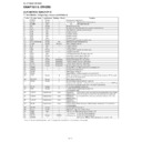
IC1 VHiLC78648E-1: CD Digital Signal Processor (LC78648E) (2/2)
In this unit, the terminal with asterisk mark (*) is (open) terminal which is not connected to the outside.
The same potential must be supplied to all power supply pins, i, e., AVDD1, AVDD2, XVDD, DVDD, LVDD and RVDD)
Pin No.
Terminal Name
Input/Output
Setting in Reset
Function
44
RCHO
Output
RVDD /2
Right channel
D/A converter
D/A converter
R channel Power supply pin.
45
RVDD
—
—
R channel output supply pin.
46
XVSS
—
—
Digital GND pin. Must always be connected to 0V
47
XOUT
Output
Oscillator
Crystal
oscillator
Power supply for crystal oscillator.
Connected for a 16.9344 MHz crystal oscillator pin.
Connected for a 16.9344 MHz crystal oscillator pin.
48
XIN
Input
Oscillator
49
XVDD
—
—
Digital power supply pin. Must always be connected to 0V
50
IOMODE
Input
—
CONT4 to 6.MONI3~5, DRF, WRQB pin output mode switching input pin.
”L” setting: Normal output “H” setting: Nch open drain output
”L” setting: Normal output “H” setting: Nch open drain output
51
F16MIN
Input
—
DF. DAC external clock input pin.
52*
OUT1
Output
L
General-purpose output pin 1.
53*
16MOUT
Output
CLK
Output
16.9344 MHz output port.
54
ASLRCK
Input
—
Anti-shock
Left/Right clock input pin.
(Must be connect to 0 V when unused.)
(Must be connect to 0 V when unused.)
55
ASDACK
Input
—
Bit clock input pin.
(Must be connect to 0 V when unused.)
(Must be connect to 0 V when unused.)
56
ASDFIN
Input
—
Left/Right channel data input pin.
(Must be connect to 0 V when unused.)
(Must be connect to 0 V when unused.)
57
LRSK
Output
L
Digital data out-
put
Left/Right channel data output pin.
58
DATACK
Output
L
Bit clock output pin.
59
DATA
Output
L
Left/Right clock output pin.
60
DVDD
—
—
Digital power supply pin.
61
DVSS
—
—
Digital GND pin 2. Must always be connected to 0V.
62
CE
Input
—
Microcomputer
Interface
Chip enable signal input pin.
63
CL
Input
—
Data transfer clock input pin.
64
DI
Input
—
Data output pin.
65
DO
Output
(H)
Data output pin. (Try state output.)
66
WRQB
Output
L
Interruption signal output pin.
67
RESB
Input
—
Reset input pin for LSI.
This pin must be set LOW briefly after power is first applied.
This pin must be set LOW briefly after power is first applied.
68
DRF
Output
L
Focus ON detection pin.
69
C2F/SBCK
Input/Output
Input
Error flag monitor pin, or sub code
read clock input pin.
read clock input pin.
Controlled by commands from the micro-
processor.
processor.
70
CONT6/SBCK
Input/Output
Input
General-purpose I/O pin 6, or sub
code read clock input pin.
code read clock input pin.
Controlled by commands from the micro-
processor.
Any of these that are unused must be either
set up as input pin ports and connected to
0V, or set up as output pin ports and left
open.
processor.
Any of these that are unused must be either
set up as input pin ports and connected to
0V, or set up as output pin ports and left
open.
71*
MONI5
Output
L
Internal signal monitor pin 5.
72*
MONI4
Output
L
Internal signal monitor pin 4.
73*
MONI3
Output
L
Internal signal monitor pin 3.
74
CONT5
Input/Output
Input
General pur-
pose I/O pin 5.
pose I/O pin 5.
Controlled by command from the microprocessor. Any of
these that are unused must be either set up as input pin
ports and connected to 0V, or set up as output pin ports and
left open when unused.
these that are unused must be either set up as input pin
ports and connected to 0V, or set up as output pin ports and
left open when unused.
75
CONT4
Input/Output
Input
General pur-
pose I/O pin 4.
pose I/O pin 4.
76
PDO1
Output
—
PLL
Phase comparison output pin 1 to control built-in VCO.
77
PDO2
Output
—
Phase comparison output pin 2 to control built-in VCO.
78
PCKIST
Input
—
Resistor connection pin to set current for PDO1 and 02 out-
puts.
puts.
79
VVSS
—
—
Built-in VCO GND pin. Must always be connected to 0V.
80
VVDD
—
—
Built-in VCO power supply pin.
XL-HP404E/HP404H
8 – 3
IC1 VHiLC78648E-1: CD Digital Signal Processor(LC78648E)
1
2
3
3
4
5
5
6
7
7
8
9
9
10
11
11
12
13
13
14
15
15
16
17
18
18
19
20
21 22 23 24 25 26 27 28 29 30 31 32 33 34 35 36 37 38 39 40
80 79 78 77 76 75 74 73 72 71 70 69 68 67 66 65 64 63 62 61
60
59
58
58
57
56
56
55
54
54
53
52
52
51
50
50
49
48
48
47
46
46
45
44
43
43
42
41
AVDD1
SLCO
EFMIN
RF
LPF
JITTC
AIN
CIN
BIN
DIN
FEC
PHLPF/RFMON
VREF
EIN
FIN
TEC
TE
TEIN
LDD
LDS
FDO
TDO
SLDO
SPDO
AVSS
AVDD2
DVDD
DVSS
VPB
DEFECT
FSEQ
EFLG
FSX
CONT1
CONT2
CONT3
MONI1
MONI2
DOUT
TEST
VVDD
VVSS
PCKIST
PD02
PD01
CONT4
CONT5
MONI3
MONI4
MONI5
CONT6/SBCK
C2F/SBCK
DRF
*RES
*WRQ
DO
DI
CL
CE
DVSS
DVDD
DATA
DATACK
LRSY
ASDFIN
ASDACK
ASLRCK
F16MOUT
OUT1
F16MIN
IOMODE
XVDD
XIN
XOUT
XVSS
RVDD
RCHO
LRVSS
LCHO
LVDD
LC78648E
PHLPF/RFMON
VREF
LDD
LDS
LDS
LPF
RF
AIN
CIN
BIN
DIN
CIN
BIN
DIN
FEC
EIN
FIN
FIN
TEC
TE
TEIN
JITTC
SLCO
EFMIN
PDO1
PDO2
PDO2
PCKIST
VVDD
VVSS
RVDD
RCHO
LRVSS
LCHO
LVDD
XVDD
XVSS
XIN
XOUT
F16MIN
F16MOUT
ASLRCK
ASDACK
ASDFIN
RESB
TEST
IOMODE
FDO
TDO
SPDO
SLDO
TDO
SPDO
SLDO
AVDD1
AVSS
AVDD2
AVSS
AVDD2
DEFECT
DRF
VPB
CONT1~6
OUT1
OUT1
FSEQ
CL
CE
DI
DO
WRQB
CE
DI
DO
WRQB
DOUT
LRSY
DATACK
DATA
DATACK
DATA
FSX
EFLG
C2F
EFLG
C2F
MONI1~5
DVDD
DVDD
DVSS
DVSS
DVDD
DVSS
DVSS
MONITOR
VREF
APC
RF SIGNAL
PROCESSOR
FOCUS ERROR
PROCESSOR
JITTER/DETECT
PLL
CLOCK
GENERATOR
EXTERNAL
AUDIO IN
LPF
SLICE LEVEL
CONTROL
TRACKING ERROR
PROCESSOR
1bit DAC
RAM
ATTENUATION
INTERPOLATION
MUTE
ERROR
CORRECTION
8FS DIGITAL
FILTER
DEEMPHASIS
SERIAL
OUT
A/D
AUTO
ADJUST
SETVO
PROCESSEROR
TRACK
JUMP
CLV
CAV
CONTROL
A/D
RAM
RUPTURE
DEFECT
DRF
CPU I/F
FRAME SYNC
DETECT,PROTECT,
INSERT,
EFMDECODE
PORT
MONITOR SIGNAL
SELECTOR
SUBCODE DECODE
CRC & TEXT
AUDIO OUT
Figure 1 BLOCK DIAGRAM OF IC
XL-HP404E/HP404H
8 – 4
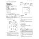
IC2 VHILA6261//-1: Focus/Tracking/Spin/Sled Driver (LA6261)
In this unit, the terminal with asterisk mark (*) is (open) terminal which is not connected to the outside.
*
Set power system GND to the minimum potential together with SGND
*
Short-circuit three pins of power system SVSS and PVCC1 externally before use.
Pin No.
Terminal Name
Function
1
VO3+
BTL Output pin (+) for channel 3.
2
VO3-
BTL Output pin (-) for channel 3.
3
VO2+
BTL Output pin (+) for channel 2.
4
VO2-
BTL Output pin (-) for channel 2.
5
VO1+
BTL Output pin (+) for channel 1.
6
VO1-
BTL Output pin (-) for channel 1.
7
PGND1
Power GND for channels 1,2,3 and 4 (BTL).
8
REGIN
Regulator pin (External PNP base).
9
PVCC1
Power for channels 1,2,3 and 4 (BTL). (SVCC short-crircuited)
10
REGOUT
Regulator pin (External PNP collector).
11
VIN1
Input pin for channel 1
12*
VIN1G
Input pin for channel 1 (for gain control)
13
VIN2
Input pin for channel 2
14*
VIN2G
Input pin for channel 2 (for gain control)
15
VIN3
Input pin for channel 3
16*
VIN3G
Input pin for channel 3 (for gain control)
17
VIN4
Input pin for channel 4
18
VIN4G
Input pin for channel 4 (for gain control)
19
FWD5
CH5 Output change pin (FWD). Logic input for bridge.
20
REV5
CH5 Output change pin (REV). Logic input for bridge.
21
VCONT5
Input pin for CH5 output voltage control
22
FWD6
CH6 Output change pin (FWD). Logic input for bridge.
23
REV6
CH6 Output change pin (REV). Logic input for bridge.
24
VCONT6
Input pin for CH5 output voltage control.
25
VREFIN
Reference voltage input pin.
26
SGND
Signal system GND
27
SVCC
Signal system power (PVCC1 short - circuited)
28
PVCC2
Power for channel 5 and 6 (H bridge).
29
MUTE
Input pin for BTL mute.
30
PGND2
Power GND for channels 5 and 6 (H bridge).
31
VO6+
H bridge Output pin (+) for channel 6.
32
VO6-
H bridge Output pin (-) for channel 6.
33
VO5+
H bridge Output pin (+) for channel 5.
34
VO5-
H bridge Output pin (-) for channel 5.
35
VO4+
BTL Output pin (+) for channel 4.
36
VO4-
BTL Output pin (-) for channel 4.
XL-HP404E/HP404H
8 – 5
IC2 VHILA6261//-1: Focus/Tracking/Spin/Sled Driver (LA6261)
1
2
3
4
5
6
7
8
9
10
11
12
13
14
15
16
17
18
36
35
34
33
32
31
30
29
28
27
26
25
24
23
22
21
20
19
+
-
+
-
+
-
+
-
+
-
+
-
+
-
+
-
+
-
+
-
11k
22k
1k
1k
1k
1k
11k
11k
11k
22k
22k
22k
-
+
-
+
Pre
D
rive
Pre
D
rive
+
-
+
-
+
-
Refcronce
voltage
DUFFER AMP
For 1/2 VCC
DUFFER AMP
For VREF
TSD
Bandgad
BTL
Mode
select
Mode
select
CH4
CH5
CH6
CH3
CH2
CH1
VOLTAGE
CONTROL AMP
Figure 2 BLOCK DIAGRAM OF IC

