Sharp SD-PX15H (serv.man19) Service Manual ▷ View online
SD-PX15H
8 – 1
Audio
SD-PX15H
Service Manual
SD-PX15H
Market
E
CHAPTER 8.
OTHER
[1] Function table of IC
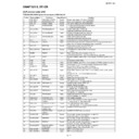
IC002 RH-iX0621AW00: System Microcomputer (IX0621AW) (1/3)
Pin No.
Terminal Name
Port Name
Input/Output
Function
1
FLD_SDATA
P96/ANEX1/SOUT4
Output
Display data output to FL driver M66005FP.
2
FLD_SCK
P95/ANEX0/CLK4
Output
Serial clock output to FL driver M66005FP.
3
FLD_CS
P94/DA1/TB4IN
Output
CS control output to FL driver M66005FP.
4
DVDa
P93/DA0/TB3IN
Output
“H”: Disc type is DVD Audio or SACD Stereo.
“L”: Other discs and functions.
“L”: Other discs and functions.
5
DVD_KDATA
P92/TB2IN/SOUT3
Output
Control data output to DVD unit.
Automatic send/receive of serial 32 bit.
Automatic send/receive of serial 32 bit.
6
DVD_DATA
P91/TB1IN/SIN3
Input
DVD/CD/VCD data input from DVD unit.
Automatic send/receive of serial 32 bit.
Automatic send/receive of serial 32 bit.
7
DVD_CLK
P90/TB0IN/CLK3
Input
Serial clock input to DVD unit.
Automatic send/receive of serial 32 bit.
Automatic send/receive of serial 32 bit.
8
BYTE
BYTE
Input
Connected to VSS since external bus is not used.
9
FLASH_VCC
CNVSS
Input
Used in the single tip mode. Connected to VSS through pull-down resis-
tance. VCC for external equipment during FLASH write.
tance. VCC for external equipment during FLASH write.
10
DVD_CS
P87/XCIN
Output
Communication start request to DVD unit.
Automatic send/receive of serial 32 bit.
Automatic send/receive of serial 32 bit.
11
RXD_CONT-IN
P86/XCOUT
Output
“H”: ROM write mode of DVD microcomputer.
“L”: Others.
“L”: Others.
12
RESET
RESET
Input
Reset input of the microcomputer. Active: “L”.
Connected to the RESET line of the writer during Flash write.
Connected to the RESET line of the writer during Flash write.
13
X_OUT
XOUT
—
Normal oscillation output of the microcomputer. 8.38 MHz crystal connec-
tion.
tion.
14
GND
VSS
—
Connected to GND (VSS).
15
X_IN
XIN
Input
Normal oscillation input of the microcomputer. 8.38 MHz crystal connection.
16
VCC
VCC
Input
Power input (3.3 V) of the microcomputer. Backup power supply.
17
FLASH “H”
P85/NMI
Input
Connected to VCC through pull-up resistance.
(Setting during FLASH write) Not used functionally.
(Setting during FLASH write) Not used functionally.
18
SYS_STOP
P84/INT2
Input
Power failure detection input. The microcomputer is shifted to the backup
mode.
Normal: “H”, “H”
mode.
Normal: “H”, “H”
→ ”L”: Power failure detection.
19
DIR_INT0
P83/INT1
Output
Auxiliary terminal
20
RX_IN
P82/INT0
Input
Sharp Type remote control input.
21
IND_TIMER
P81/TA4IN/U
Output
Timer stand-by LED control.
“H” output: LED on, “L” output: LED off
“H” output: LED on, “L” output: LED off
22
W-CONT_DATA
P80/TA4OUT/U
Output
Wireless mode: Control DATA OUT.
Others: Fixed to low output.
Others: Fixed to low output.
23
DVD_MUTE
P77/TA3IN
Input
DVD unit MUTE indication input.
“L”: MUTE_ON, “H”: MUTE_OFF
“L”: MUTE_ON, “H”: MUTE_OFF
24
DVD_PROT
P76/TA3OUT
Input
DVD power supply error detection input.
“H”: Normal, “L”: Abnormal
“H”: Normal, “L”: Abnormal
25
H.P_SW
P75/TA2IN/W
Input
Headphone insertion SW detection input.
“H”: H.P. insertion, “L”: No H.P.
“H”: H.P. insertion, “L”: No H.P.
26
FAN_LOCK
P74/TA2OUT/W
Input
FAN rotation detection.
27
NON_PCM
P73/CTS2/RTS2/
TA1IN/V
TA1IN/V
Input
Input to detect whether an audio signal is PCM.
“L”: Audio PCM, “H”: Non audio PCM
“L”: Audio PCM, “H”: Non audio PCM
28
PWD_DW
P72/CLK2/TA1OUT/
V
V
Output
1 bit AMP stand-by control output.
“L”: Stand-by mode, “H”: Normal operation mode
“L”: Stand-by mode, “H”: Normal operation mode
29
DIR_SCL
P71/RXD2/SCL/
TA0IN/TB5IN
TA0IN/TB5IN
Output
AK4586 I2C BUS clock output.
30
DIR_SDA
P70/TXD2/SDA/
TA0OUT
TA0OUT
Input/Output
AK4586B I2C BUS data input/output.
31
FLASH_TXD
P67/TXD1
Output
Functionally not used. Normally fixed to output “L”.
(Send data output to Flash Writer.)
(Send data output to Flash Writer.)
32
FLASH_RXD
P66/RXD1
Output
Functionally not used. Normally fixed to output “L”.
(Receive data input to Flash Writer.)
(Receive data input to Flash Writer.)
33
FLASH_SCLK
P65/CLK1
Output
Functionally not used. Normally fixed to output “L”.
(Transfer clock input from Flash Writer.)
(Transfer clock input from Flash Writer.)
34
FLASH_BUSY
P64/CTS1/RTS1/
CTS0/CLKS1
CTS0/CLKS1
Output
Functionally not used. Normally fixed to output “L”.
(BUSY output to Flash Writer. BUSY: “H”)
(BUSY output to Flash Writer. BUSY: “H”)
35
DSP_SCDIN
P63/TXD0
Output
DSP IC serial data output.
36
DSP_SCDOUT
P62/RXD0
Input
DSP IC serial data input.
SD-PX15H
8 – 2
IC002 RH-iX0621AW00: System Microcomputer (IX0621AW) (2/3)
In this unit, the terminal with asterisk mark (*) is (open) terminal which is not connected to the outside.
Pin No.
Terminal Name
Port Name
Input/Output
Function
37
DSP_SCCLK
P61/CLK0
Output
DSP IC serial send/receive synchronization clock output.
38
DSP_CS
P60/CTS0/RTS0
Output
DSP IC serial send/receive strobe output.
39*
OSC_OUT
P57/RDY/CLKOUT
Output
For checking main clock oscillating frequency.
With clock OUT function activated, set to f32.
With clock OUT function activated, set to f32.
40
DSP_RESET
P56/ALE
Output
DSP IC RESET output.
41
FLASH_EPM
P55/HOLD
Input
Connected to VSS through pull-down resistance.
(Setting during FLASH write) Not used functionally.
(Setting during FLASH write) Not used functionally.
42
DSP_UC15
P54/HLDA
Output
External ROM for DSP download program.
Page select output.
Page select output.
43
DSP_UC16
P53/BCLK
Output
External ROM for DSP download program.
Page select output.
Page select output.
44
DSP_UC17
P52/RD
Output
External ROM for DSP download program.
Page select output.
Page select output.
45
DSP_ABOOT
P51/WRH/BHE
Output
DSP AUTO BOOT control unit. AUTO BOOT starts by setting to “L” during
DSP RESET.
DSP RESET.
46
FLASH_CE
P50/WRL/WR
Input
Connected to VSS through pull-down resistance.
(Setting during FLASH write) Not used functionally.
(Setting during FLASH write) Not used functionally.
47
ROM
P47/CS3
Output
ROM/RAM enable control output on DSP PWB.
H: SRAM enable, L: ROM enable.
H: SRAM enable, L: ROM enable.
48*
CH_SEL1
P46/CS2
Output
Wireless channel switching output.
49*
CH_SEL2
P45/CS1
Output
Wireless channel switching output
50*
CH_SEL3
P44/CS0
Output
Wireless channel switching output
51
TRI-STATE
P43/A19
Output
1 bit AMP output stage FET control output.
“H”: Normal operation, “L”: Output stop
“H”: Normal operation, “L”: Output stop
52
VOL_DATA
P42/A18
Output
Data output for electronic Vol IC control signal.
53
VOL_STB
P41/A17
Output
Latch output for electronic Vol IC control signal.
54
VOL_CLK
P40/A16
Output
Clock output for electronic Vol IC control signal.
55
DOOR_SPED
P37/A15
Output
DVD/CD door operation speed switching output (auxiliary).
L: Low speed operation, H: High speed operation.
L: Low speed operation, H: High speed operation.
56
DOOR_M+
P36/A14
Output
Control output for CD/DVD mechanic door OPEN/CLOSE control motor.
57
DOOR_M-
P35/A13
Output
Control output for CD/DVD mechanic door OPEN/CLOSE control motor.
58
MAIN_RELAY
P34/A12
Output
Primary power supply relay control output.
“H” output: Relay ON, “L” output: Relay OFF
“H” output: Relay ON, “L” output: Relay OFF
59
DOOR_OP
P33/A11
Input
CD/DVD mechanical door OPEN SW input.
“L”: OPEN SW ON, “H”: OPEN SW OFF
“L”: OPEN SW ON, “H”: OPEN SW OFF
60
DOOR_CL
P32/A10
Input
CD/DVD mechanical door CLOSE SW input.
“L”: CLOSE SW ON, “H”: CLOSE SW OFF
“L”: CLOSE SW ON, “H”: CLOSE SW OFF
61
A/D_RESET
P61/A9
Output
1 bit AMP section
IC reset control output.
“L” output: Normal operation, “H” output: RESET
62
VCC
VCC
Input
Microcomputer’s power input (3.3 V). Backup power supply.
63
POWER_KEY
P30/A8(/-/D7)
Input
POWER button input.
“L”: POWER button ON, “H”: POWER button OFF
“L”: POWER button ON, “H”: POWER button OFF
64
GND
VSS
—
Connected to GND (VSS).
65
L-MUTE
P27/A7(/D7/D6)
Output
VTR OUT audio MUTE output.
“H”: MUTE OFF, “L”:MUTE ON
“H”: MUTE OFF, “L”:MUTE ON
66
CONFIG
P26/A6(/D6/D5)
Output
Config setting output terminal.
“H”: Config 1, “L”: Config 2
“H”: Config 1, “L”: Config 2
67
FUNC_DVD
P25/A5(/D5/D4)
Output
Power supply control to DVD unit and DIG signal switching output.
During DVD/CD FUNC: “H” output, others, “L” output.
During DVD/CD FUNC: “H” output, others, “L” output.
68
N.C.
P24/A4(/D4/D3)
Output
Not used. Set as an output terminal and fixed to Low.
69
FUNC_DIG
P23/A3(/D3/D2)
Output
“H” output: AUX, TV digital function
“L” output: Other functions
“L” output: Other functions
70
VIDEO_MUTE
P22/A2(/D2/D1)
Output
VIDEO mute control output.
“L” output: Mute on, “H” output: Mute off.
“L” output: Mute on, “H” output: Mute off.
71
SP_RELAY
P21/A1(/D1/D0)
Output
Speaker relay output.
“H” output: relay ON and energized, “L” output: relay OFF
“H” output: relay ON and energized, “L” output: relay OFF
72
H.P_MUTE
P20/A0(/D0/-)
Output
Headphone sound MUTE control output.
“L” output: MUTE ON, “H” output: MUTE OFF
“L” output: MUTE ON, “H” output: MUTE OFF
73
TH-WAR
P17/D15/INT5
Input
1 bit AMP thermal warning detection input.
“L”: Abnormal, “H”: Normal
“L”: Abnormal, “H”: Normal
74
DSP_INTREQ
P16/D14/INT4
Input
DSP data receive request signal input.
“L”: DSP to microcomputer DATA receive request
“L”: DSP to microcomputer DATA receive request
75
FAULT
P15/D13/INT3
Input
1 bit AMP error detection input.
“L”: Abnormal, “H”: Normal
“L”: Abnormal, “H”: Normal
SD-PX15H
8 – 3
IC002 RH-iX0621AW00: System Microcomputer (IX0621AW) (3/3)
Pin No.
Terminal Name
Port Name
Input/Output
Function
76
BASS_SW
P14/D12
Output
Subwoofer amplifier gain control output.
“H” output: BASS OFF, “L” output: BASS ON
“H” output: BASS OFF, “L” output: BASS ON
77
LED
P13/D11
Output
Lighting LED control. On: H, Off: L
78
FL+B
P12/D10
Output
FL power supply control output. “H”: Power ON, “L”: Power OFF
79
F-MUTE
P11/D9
Output
Front channel MUTE control output.
“L” output: MUTE ON, “H” output: MUTE OFF
“L” output: MUTE ON, “H” output: MUTE OFF
80
C-MUTE
P10/D8
Output
Center channel MUTE control output.
“L” output: MUTE ON, “H” output: MUTE OFF
“L” output: MUTE ON, “H” output: MUTE OFF
81
SW-MUTE
P07/D7
Output
Subwoofer channel MUTE control output.
“L” output: MUTE ON, “H” output: MUTE OFF
“L” output: MUTE ON, “H” output: MUTE OFF
82
SR-MUTE
P06/D6
Output
Surround channel MUTE control output.
“L” output: MUTE ON, “H” output: MUTE OFF
“L” output: MUTE ON, “H” output: MUTE OFF
83
AUDITION
P05/D5
Input
Audition model selection input.
“H”: Audition model, “L”: Normal model
“H”: Audition model, “L”: Normal model
84
FM_STB
P04/D4
Output
“L”: Function is FM stereo or FM mono
“H”: Others
“H”: Others
85
CCB_DO
P03/D3
Input
Serial data input from Sanyo CCB Device.
86
CCB_CL
P02/D2
Output
Serial clock output from Sanyo CCB Device.
87
CCB_DI
P01/D1
Output
Serial command data input from Sanyo CCB Device.
88
CCB_CE
P00/D0
Output
CE control output to Sanyo CCB Device.
89
TUN_SM
P107/AN7/KI3
Input
A/D capture. Tuner electric intensity comparison detection input.
Used only for international RDS function. Fixed to national VSS level.
Used only for international RDS function. Fixed to national VSS level.
90
+B_CHECK
P106/AN6/KI2
Input
A/D capture. Power ON detection port.
91
PROTECT
P105/AN5/KI1
Input
A/D capture. System error detection input.
92
AREA
P104/AN4/KI0
Input
A/D capture. Local settings for TUNER BAND.
93
JOG
P103/AN3
Input
A/D capture. JOG rotation detection input.
94
DOOR_PROT
P102/AN2
Input
Detection input of “catching-finger in CD/DVD mechanic door”.
Abnormal load detection by A/D download.
Abnormal load detection by A/D download.
95
KEY2
P101/AN1
Input
A/D import, main unit key input 2. Only Power key is connected.
96
AVSS
AVSS
—
VSS terminal for A/D converter. Connected to GND (VSS).
97
KEY1
P100/AN0
Input
A/D import, main unit key input 1.
98
VREF
VREF
Input
Reference voltage input terminal of A/D converter.
99
AVCC
AVCC
Input
Power input terminal of A/D converter. Connected to VCC.
100
FLD_RESET
P97/ADTRG/SIN4
Input
Reset output to FL driver M66005FP.
SD-PX15H
8 – 4
IC413 VHiM61531FP-1: 6-ch VR Driver (M61531FP) (1/2)
In this unit, the terminal with asterisk mark (*) is (open) terminal which is not connected to the outside.
Pin No.
Terminal Name
Function
1
INR3
Rch input terminal (input selector).
2
INL2
Lch input terminal (input selector).
3
INR2
Rch input terminal (input selector).
4
INL1/EXT INL
Lch input terminal (input selector)/External input terminal (Lch).
5
INR1/EXT INR
Rch input terminal (input selector)/External input terminal (Lch).
6
GND
Analog GND terminal.
7
CIN1
Cch input terminal (2 input selectors).
8
SWIN1
SWch input terminal (2 input selectors).
9
SRIN1
SRch input terminal (2 input selectors).
10
SLIN1
SLch input terminal (2 input selectors).
11
LIN1
Lch input terminal (2 input selectors).
12
RIN1
Rch input terminal (2 input selectors).
13
GND
Analog GND terminal.
14*
BALANCE L/+
Lch balance output (+) terminal.
15*
LOUD L/BALANCE L/-
Loudness frequency characteristic setting terminal/Lch balance output (-) terminal.
16
GND
Analog GND terminal.
17*
BALANCE R/+
Rch balance output (+) terminal.
18*
LOUD R/BALANCE R/- Loudness frequency characteristic setting terminal/Rch balance output (-) terminal.
19
GND
Analog GND terminal.
20
LIN2
Lch input terminal (2 input selectors).
21
RIN2
Rch input terminal (2 input selectors).
22
SRIN2
SRch input terminal (2 input selectors).
23
SLIN2
SLch input terminal (2 input selectors).
24
CIN2
Cch input terminal (2 input selectors).
25
SWIN2
SWch input terminal (2 input selectors).
26
DGND
Internal logic circuit. GND terminal.
27
CLOCK
CLOCK input terminal for transferring serial data.
28
DATA
DATA input terminal for transferring serial data.
29
LATCH
LAYCH input terminal for transferring serial data.
30
DVDD
Internal logic circuit. Power supply terminal.
31
AVCC
Internal logic circuit. Positive power supply terminal.
32
GND
Analog GND terminal.
33
SWSELOUT
SWch volume input selector. Output terminal.
34
SWVIN
SWch volume input terminal.
35
SWOUT
SWch output terminal.
36
COUT
Cch output terminal.
37
CVIN
Cch volume input terminal.
38
CSELOUT
Cch volume input selector. Output terminal.
39
SLSELOUT
SLch volume input selector. Output terminal.
40
SLVIN
SLch volume input terminal.
41
SLOUT
SLch output terminal.
42
SROUT
SRch output terminal.
43
SRVIN
SRch volume input terminal.
44
SRSELOUT
SRch volume input selector. Output terminal.
45
RSELOUT
Rch volume input selector. Output terminal.
46
RVIN
Rch volume input terminal.
47
ROUT
Rch output terminal.
48
TRE R
Tone control (treble) frequency characteristic setting terminal.
49
BASS R2
Tone control (bass) frequency characteristic setting terminal.
50
BASS R1
Tone control (bass) frequency characteristic setting terminal
51
BASS L2
Tone control (bass) frequency characteristic setting terminal
52
BASS L1
Tone control (bass) frequency characteristic setting terminal
53
TRE L
Tone control (treble) frequency characteristic setting terminal.
54
LOUT
Lch output terminal.
55
LVIN
Lch volume input terminal.
56
LSELOUT
Lch volume input selector. Output terminal.
57
GND
Analog GND terminal.
58
RECL1
REC output terminal (Lch).
59
RECR1
REC output terminal (Rch).
60
RECL2
REC output terminal (Lch).
61
RECR2
REC output terminal (Rch).
62*
RECL3
REC output terminal (Lch).

