Sharp SD-EX200 (serv.man18) Service Manual ▷ View online
SD-EX200H
– 42 –
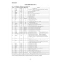
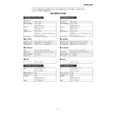
FUNCTION TABLE OF IC
IC1 VHiLC78646E-1: CD Servo (LC78646E) (1/2)
1
SLCO
Output
—
Control output.
2
SLCIST
Input
—
Resistor connection terminal for SLCO output current setting.
3
EFMIN
Input
—
RF signal input terminal.
4
RF
Output
—
RF signal monitor terminal.
5
RFVDD
Input
—
RF power terminal.
6
RFVSS
—
—
RF earth terminal. To be connected to 0 V.
7
FIN1
Input
—
A+C signal input terminal.
8
FIN2
Input
—
B+D signal input terminal.
9
TIN1
Input
—
E signal input terminal.
10
TIN2
Input
—
F signal input terminal.
11
VREF
Output
RFVDD/2
VREF voltage output terminal.
12
REF1
Input
—
Reference supply setting terminal.
13*
FE
Output
ZHI
FE signal monitor terminal.
14
TEC
Output
—
LPF capacitor connection terminal for TE signal.
15*
TE
Output
ZHI
TE signal monitor terminal.
16*
RFMON
Output
ZHI
RF internal signal monitor terminal.
17
JITTC
—
—
Capacitor connection terminal for jitter detection.
18
ADAVDD
Input
—
Power terminal for servo A/D, D/A.
19
ADAVSS
—
—
Earth terminal for serve A/D, D/A. To be connected to 0 V.
20
TDO
Output
ADAVDD/2
Output terminal for tracking control. D/A output.
21
FDO
Output
ADAVDD/2
Output terminal for focus control. D/A output.
22
SPDO
Output
ADAVDD/2
Output terminal for spindle control. D/A output.
23
SLDO
Output
ADAVDD/2
Output terminal for sled control. D/A output.
24*
GPDAC
Output
ADAVDD/2
Servo D/A general-purpose output terminal.
25
CONT4
Input/Output
Input Mode
General-purpose I/O terminal 4.
26
CONT5
Input/Output
Input Mode
General-purpose I/O terminal 5.
27*
SBCK/CONT6
Input/Output
Input Mode
General-purpose I/O terminal 6 or
Subcode reading clock input terminal.
Subcode reading clock input terminal.
28
SBCK/FG
Input
—
Subcode reading clock input terminal/FG signal input terminal/external
emphasis setting terminal. Terminal functions are set by commands. When
not used, connect to 0 V.
emphasis setting terminal. Terminal functions are set by commands. When
not used, connect to 0 V.
29*
DEFECT
Output
L
Defect terminal.
30*
V/*P
Output
H
Auto switching monitor output terminal for rough servo phase control. “H”:
rough servo, “L”: phase servo.
rough servo, “L”: phase servo.
31*
FSEQ
Output
L
Sync signal detection output terminal.
The status changes to “H” when the sync signal detected in EFM and the
sync signal of internal generation are identified.
The status changes to “H” when the sync signal detected in EFM and the
sync signal of internal generation are identified.
32*
MONI1
Output
L
Internal signal monitor terminal 1.
33*
MONI2
Output
L
Internal signal monitor terminal 2.
34
DE_EMPH
Output
L
Internal signal monitor terminal 3.
35*
MONI4
Output
L
Internal signal monitor terminal 4.
36*
MONI5
Output
L
Internal signal monitor terminal 5.
37
VSS
—
—
Digital system earth terminal. To be connected to 0 V.
38
VDD
Input
—
Digital system power terminal.
39
DOUT
Output
L
Digital OUT output terminal. (EIAJ format)
40
TEST
Input
L
Input terminal for test. To be connected to 0 V.
41
LVDD
Input
—
Power supply for Left channel.
42*
LCHO
Output
LVDD/2
Left channel output.
43
LVSS
—
—
GND for Left channel. Must be connected to 0 V.
Pin No.
Function
Terminal Name Input/Output Setting in Reset
In this unit, the terminal with asterisk mark (*) is (open) terminal which is not connected to the outside.
Left channel
D/A converter
For slice level
control.
Controlled by commands from the
microcomputer. When not used, set
them as input terminals and connect
to 0 V, or set them as output
terminals and leave open.
microcomputer. When not used, set
them as input terminals and connect
to 0 V, or set them as output
terminals and leave open.
– 43 –
SD-EX200H
IC1 VHiLC78646E-1: CD Servo (LC78646E) (2/2)
44
RVSS
—
—
GND for Right channel. Must be connected to 0 V.
45*
RCHO
Output
LVDD /2
Right channel output.
46
RVDD
Input
—
Power supply for Right channel.
47
XVDD
Input
—
Power supply for crystal oscillator.
48
XOUT
Output
—
Connected for the 33.8688 MHz crystal oscillator cement.
49
XIN
Input
—
50
FSX/16MIN
Input/Output
Input
7.35 kHz Synchronization signal monitor port.
or Clock input port for Digital filter & D/A
or Clock input port for Digital filter & D/A
51
XVSS
—
—
Crystal
GND for crystal oscillator. Must be connected to 0 V.
Oscillator
52*
C2F
Output
H
C2 FLAG monitor port.
53*
EFLG
Output
L
C1, C2 error corrected monitor port.
54
16MOUT
Output
Clock
16.9344 MHz output port.
55
ASLRCK
Input
—
Word clock input port.
(If this port does not use, must be connect to 0 V.)
(If this port does not use, must be connect to 0 V.)
56
ASDACK
Input
—
Bit clock input port.
(If this port does not use, must be connect to 0 V.)
(If this port does not use, must be connect to 0 V.)
57
ASDFIN
Input
—
Left/Right channel data input port.
(If this port does not use, must be connect to 0 V.)
(If this port does not use, must be connect to 0 V.)
58
LRCK
Output
L
Word clock output port.
59
BCK
Output
L
Digital data
Bit clock output port.
60
DATA
Output
L
Left/Right channel data output port.
61
CE
Input
—
Chip enable signal input port.
62
CL
Input
—
Microcomputer
Data transfer clock input port.
63
DI
Input
—
Interface
Data input port.
64
DO
Output
(H)
Data output port. (N-ch. open drain output.)
65
*WRQ
Output
H
Interruption signal output.
66
*RES
Input
—
Chip reset signal input port.
This port must be set LOW after first applied power on.
This port must be set LOW after first applied power on.
67
DRF
Output
L
Focus detection output port.
68
VDD5
Input
—
Power supply for Microprocessor.
69
VSS
—
—
GND for digital circuit. Must be connected to 0 V.
70
CONT3
Input/Output
Input
General purpose port 1.
71
CONT2
Input/Output
Input
General purpose port 2.
72
CONT1
Input/Output
Input
General purpose port 3.
73
PDO1
Output
—
Internal VCO control phase comparator output port 1.
74
PDO2
Output
Input
Internal VCO control phase comparator output port 2.
75
VVSS
—
—
GND for internal VCO. Must be connected to 0 V.
76
PCKIST
Input
—
PDO output current adjustment resistor connection port.
77
VVDD
Input
—
Power supply for internal VCO.
78
FR
Input
—
VCO frequency range adjustment port.
79
LDS
Input
—
LASER power detected signal input port.
80
LDD
Output
—
LASER power control signal output port.
Pin No.
Function
Terminal Name Input/Output Setting in Reset
Right channel
D/A converter
D/A converter
Crystal
Oscillator
Anti-shock
Controlled with serial data command from micro-
computer. When not used, General purpose input/
output terminal 7. Set it as the input terminal and open
it by connecting to 0 V, or set it as the output terminal
and open it.
computer. When not used, General purpose input/
output terminal 7. Set it as the input terminal and open
it by connecting to 0 V, or set it as the output terminal
and open it.
PLL
In this unit, the terminal with asterisk mark (*) is (open) terminal which is not connected to the outside.
Be sure to supply the same potential to each power terminal. (VVDD, ADAVDD, VDD, LVDD, RVDD, XVDD)
Terminal witch is controlled by the power terminal (VDD5 V) for a microcomputer interface :
CE (61 pin), CL (62 pin), DI (63 pin), DO (64 pin), WRQ (65 pin), RES (66 pin), DRF (67 pin)
Terminal witch is controlled by the power terminal (VDD5 V) for a microcomputer interface :
CE (61 pin), CL (62 pin), DI (63 pin), DO (64 pin), WRQ (65 pin), RES (66 pin), DRF (67 pin)
SD-EX200H
– 44 –
Figure 44 BLOCK DIAGRAM OF IC
IC1 VHiLC78646E-1: CD Servo (LC78646E)
1
2
3
4
5
6
7
8
9
10
11
12
13
14
15
16
17
18
19
20
21
22
23
24
25
26
27
28
29 30
31
32
33
34
35 36
37
38
39
40
80
79
78
77
76
75
74
73
72 71
70
69
68
67
66 65
64
63
62
61
60
59
58
57
56
55
54
53
52
51
50
49
48
47
46
45
44
43
42
41
SLCO
SLCIST
EFMIN
RF
RFVDD
RFVSS
FIN1
FIN2
TIN1
TIN2
VREF
REF1
FE
TEC
TE
RFMON
JITTC
ADAVDD
ADAVSS
TDO
FDO
SPDO
SLDO
GPDAC
CONT4
CONT5
SBCK/CONT6
SBCK/FG
DEFECT
V/*P
FSEQ
MONI1
MONI2
MONI3
MONI4
MONI5
(3.3V)VSS
VDD
DOUT
TEST
LDD
LDS
FR
VVDD
PCKIST
VVSS
PD02
PD01
CONT1
CONT2
CONT3
VSS
VDD5
DRF
*RES
*WRQ
DO
DI
CL
CE
DATA
BCK
LRCK
ASDFIN
ASDACK
ASLRCK
16MOUT
EFLG
C2F
XVSS
FSX/16MIN
XIN
XOUT
XVDD
RVDD
RCHO
RVSS
LVSS
LCHO
LVDD
LC78646E
+
–
+
–
+
–
+
–
–
–
+
+
MIX
LPF
LPF
LPF
TBAL
TBAL
RAM
LEVEL SET
AGC
EQ
SW
PH
BH
+
–
+
–
+
–
+
–
MONI
CONT
A/D
SERVO PROCESSOR
TRACK JUMP
AUTO ADJUST
JITTER
DETECT
1bit DAC
8FS
DIGITAL FILTER
GENERAL-PURPOSE
PORTS
COMMAND
INTERFACE
CLOCK
GENERATOR
CLV,CAV
CONTROL
PLL
VCEC
SLICE LEVEL
CONTROL
APC
S/H
D/A
SW
DRF
RUPTURE DEFECT
FRAME SYNC
DETECT,PROTECT INSERT,
EFN DECODE
VDD
SUBCODE DECODE CRC
MONITOR SIGNAL SELECTOR
RAM
ERROR
CORRECTION
AUDIO CD
AUDIO OUT
SERIAL
OUT
EXTERNAL
AUDIO IN
INTERPOLATION
MUTE
ATTENUATION
DEEMPHSIS
LPF
FIN1
FIN2
TIN1
TIN2
REF1
DETECT
ADIN
ADAVDD
ADAVSS
JITTC
SLCO
EFMIN
SLCIST
PCK
PDO1
PDO2
PDO2
FR
PCKIST
VVDD
VVSS
SBCK/FG
XIN
XOUT
16MOUT
XVDD
XVSS
*RES
*WRQ
CL
CE
DI
DO
VDD5V
CONT1, 2, 3
TEST
CONT4, 5
SBCK/CONT6
LVDD
LVSS
LCHO
RCHO
RVDD
RVSS
ASDFIN
ASDQCK
ASLRCK
DATA
BCK
LRCK
DOUT
EFLG
C2F
FSK/16MIN
MONI1~5
VSS
VDD
V/*P
FSEQ
DRF
GPDAC
SPD0
SLD0
TD0
FD0
LDS
LDD
VREF
RFMON
RFVSS
RFVDD
RF
TEC
TE
FE
– 45 –
SD-EX200H
IC101 VHiCS4340KS-1: DAC IC (CS4340KS) (1/2)
1
RST
Input
Reset
The device enters a low power mode and all internal state machines are reset to the default
settings when low. RST should be held low during power-up until the power supply, master
and left/right clocks are stable.
The device enters a low power mode and all internal state machines are reset to the default
settings when low. RST should be held low during power-up until the power supply, master
and left/right clocks are stable.
2
SDATA
Input
Serial Audio Data
Two's complement MSB-first serial data is input on this pin. The data is clocked into SDATA
via the serial clock and the channel is determined by the Left/Right clock.
The required relationship between the Left/Right clock, serial clock and serial data is defined
by the DIF1-0 pins.
Two's complement MSB-first serial data is input on this pin. The data is clocked into SDATA
via the serial clock and the channel is determined by the Left/Right clock.
The required relationship between the Left/Right clock, serial clock and serial data is defined
by the DIF1-0 pins.
3
SCLK
Input
Serial Clock
Clocks the individual bits of the serial data into the SDATA pin.
The required relationship between the Left/Right clock, serial clock and serial data is defined
by the DIF1-0 pins.
The CS4340 supports both internal and external serial clock generation modes.
Internal SCLK mode is used to gain access to extra de-emphasis modes.
Internal Serial Clock Mode
In the internal Serial Clock Mode, the serial clock is internally derived and synchronous with
the master clock and left/right clock.
The SCLK/LRCK frequency ratio is either 32, 48 or 64 depending upon the DIF1-0 pins.
Operation in this mode is identical to operation with an external serial clock synchronized with
LRCK.
External Serial Clock Mode
The CS4340 will enter the External Serial Clock Mode whenever 16 low to high transitions
are detected on the SCLK pin during any phase of the LRCK period.
The device will revert to Internal Serial Clock Mode if no low to high transitions are detected
on the SCLK pin for 2 consecutive periods of LRCK.
DEM1
Input
De-emphasis Control
Implementation of the standard 15
Implementation of the standard 15
µ
s/50
µ
s digital de-enphasis filter response, required
reconfiguration of the digital filter to maintain the proper filter response for 32, 44.1 or 48 kHz
sample rates.
When using Internal Serial Clock Mode, as described above, Pin 3 is available for de-emphasis
control, DEM1, and all de-enphasis filters are available.
When using External Serial Clock Mode, as described above, Pin 3 is not available for
de-emphasis use and only the 44.1 kHz de-emphasis filter is available.
Note: De-emphasis is not available in High-Rate Mode.
4
LRCK
Input
Left/Right Clock
The Left/Right clock determines which channel is currently being input on the serial audio
data input, SDATA. The frequency of the Left/Right clock must be at the input sample rate.
Audio samples in Left/Right sample pairs will be simultaneously output from the digital- to-
analog converter whereas Right/Left pairs will exhibit a one sample period difference.
The required relationship between the Left/Right clock, serial clock and serial data is defined
by the DIF1-0 pins.
5
MCLK
Input
Master Clock
The master clock frequency must be either 256x, 384x or 512x the input sample rate in Base
Rate Mode (BRM) and either 128x or 129x the input sample rate in High Rate Mode (HRM).
The master clock frequency must be either 256x, 384x or 512x the input sample rate in Base
Rate Mode (BRM) and either 128x or 129x the input sample rate in High Rate Mode (HRM).
Pin No.
Port Name
Input/Output
Function
Sample
Rate
(kHz)
MCLK (MHz)
HRM
BRM
128x
192x
256x
384x
512x
32
4.0960
6.1440
8.1920
12.2880
16.3840
44.1
5.6448
8.4672
11.2896
16.9344
22.5792
48
6.1440
9.2160
12.2880
18.4320
24.5760
64
8.1920
12.2880
—
—
—
88.2
11.2896
16.9344
—
—
—
96
12.2880
18.4320
—
—
—
Common Master Clock Frequencies
DEM1
DESCRIPTION
0
Disabled
0
44.1 kHz
1
48 kHz
1
32 kHz
Internal Serial Clock Mode

