Sharp SD-EX100H (serv.man18) Service Manual ▷ View online
SD-EX100H
– 66 –
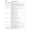
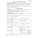
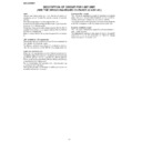
FUNCTION TABLE OF IC
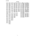
IC60 VHiLC72131/-1: PLL (Tuner) (LC72131)
1
XIN
Connection of crystal (4.5 MHz/7.2 MHz).
2*
VSSX
Ground terminal of LC72121 crystal oscillation circuit system.
3
CE
To obtain high level during serial data input (DI) to LC72121 and during serial data output (DO).
4
DI
Input terminal for serial data to be transferred from controller to LC72121.
5
CL
Clock for synchronizing with data during serial data input (DI) to LC72121 and during serial data
output (DO).
output (DO).
6
DO
To output data from LC72121 to controller. Contents of output data determined according to
serial data DOC0 to DOC2.
serial data DOC0 to DOC2.
7,8,9,10
BO1-BO4
Terminal exclusively for output.
Output state determined by serial data BO1 to BO4.
"Data" = 0: Open; "Data" = 1: "L"
Time base signal (8 Hz) output from BO1 terminal possible (Serial data set at TBC = "1").
Output state determined by serial data BO1 to BO4.
"Data" = 0: Open; "Data" = 1: "L"
Time base signal (8 Hz) output from BO1 terminal possible (Serial data set at TBC = "1").
11
IO1
Input-output terminal.
Input-output determined by serial data IOC1 and IOC2.
"Data" = 0: Input port; "Data" = 1: Output port
When designated as input port.
Input terminal state transmitted from DO terminal to controller.
"Input state" = "L": Data
Input-output determined by serial data IOC1 and IOC2.
"Data" = 0: Input port; "Data" = 1: Output port
When designated as input port.
Input terminal state transmitted from DO terminal to controller.
"Input state" = "L": Data
0, "H": Data
1
When designated as output port.
Output state determined by serial data IO1 and IO2.
"Data" = 0: Open, 1: "L"
Input port obtained during power ON and reset.
Output state determined by serial data IO1 and IO2.
"Data" = 0: Open, 1: "L"
Input port obtained during power ON and reset.
12
IFIN
Input frequency: 0.4 – 12 MHz
Signals directly transmitted to IF counter.
Results output from MSB of IF counter via DO.
4 Types of measuring time (4,8,32,and 64 ms).
Signals directly transmitted to IF counter.
Results output from MSB of IF counter via DO.
4 Types of measuring time (4,8,32,and 64 ms).
13
IO2
Input-output terminal.
Input-output determined by serial data IOC1 and IOC2.
"Data" = 0: Input port, "Data" = 1: Output port
When designated as input port.
Input terminal state transmitted from DO terminal to controller.
"Input state" = "L": Data
Input-output determined by serial data IOC1 and IOC2.
"Data" = 0: Input port, "Data" = 1: Output port
When designated as input port.
Input terminal state transmitted from DO terminal to controller.
"Input state" = "L": Data
0, "H": Data
1
When designated as output port.
Output state determined by serial data IO1 and IO2.
Data = 0: Open, 1: "L"
Input port obtained during power ON and reset.
Output state determined by serial data IO1 and IO2.
Data = 0: Open, 1: "L"
Input port obtained during power ON and reset.
14*
VSSd
Ground terminal for digital systems except for VSSa and VSSX of LC72121.
15
AMIN
Serial data input: In case of DVS = 0, AMIN is selected.
Serial data input: In case of SNS = 1
• Input frequency: 2 – 40 MHz.
• Signals directly transmitted to swallow counter.
• Set divided value: 272 – 65,535. Actual divided value is as specified.
Serial data input: In case of SNS = 0
• Input frequency: 0.5 – 10 MHz
• Signals directly transmitted to 12 bits programmable divider.
• Set divided value: 4 – 4,095. Actual divided value is as specified.
16
FMIN
Serial data input: In case of DVS = 1, FMIN selected.
Input frequency: 10 – 160 MHz
Signals directly transmitted to swallow counter via built-in prescaler (1/2).
Set divided value: 272 – 65,535. Actual divided value double the set value by built-in prescaler
(1/2).
Input frequency: 10 – 160 MHz
Signals directly transmitted to swallow counter via built-in prescaler (1/2).
Set divided value: 272 – 65,535. Actual divided value double the set value by built-in prescaler
(1/2).
17
VDD
Power supply terminal for LC72121 (VDD = 2.7 – 3.6 V).
When supplying power, power-ON reset circuit operates.
When supplying power, power-ON reset circuit operates.
18
PD
Charge pump output terminal for PLL.
If frequency is higher than the reference frequency when local oscillation signal frequency is
divided by N: Level "H" output from PD terminal.
If lower: Level "L" output. If agreed with the reference frequency: High impedance.
If frequency is higher than the reference frequency when local oscillation signal frequency is
divided by N: Level "H" output from PD terminal.
If lower: Level "L" output. If agreed with the reference frequency: High impedance.
19,20
AIN, AOUT
Nch MOS transistor for PLL active low-pass filter.
21
VSSa
MOS Transistor ground terminal for LC72121 low-pass filter.
22
XOUT
Connection of crystal (4.5 MHz/7.2 MHz).
—
NC
Nothing connected
Pin
No.
No.
Function
Terminal Name
In this unit, the terminal with asterisk mark (*) is (open) terminal which is not connected to the outside.
– 67 –
SD-EX100H
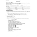
IC60 VHiLC72131/-1: PLL (Tuner) (LC72131)
IC30 VHiLA1832S/-1: FM IF Det./FM Mpx./AM IF (LA1832S)
XIN
XOUT
FMIN
AMIN
CE
DI
CL
DO
VDD
VSSd
POWER
ON
RESET
CCB
I/F
I/F
1/2
REFERENCE
DIVIDER
DIVIDER
SWALLOW COUNTER
1/16, 1/17, 4bits
1/16, 1/17, 4bits
12bits PROGRAMMABLE
DIVIDER
DIVIDER
DATA SHIFT REGISTER
LATCH
UNIVERSAL
COUNTER
COUNTER
UNLOCK
DETECTOR
DETECTOR
PHASE DETECTOR
CHARGE PUMP
CHARGE PUMP
BO1 BO2 BO3 BO4
IO1
IO2
PD
AIN
AOUT
IFIN
3
4
5
1
7
8
9
6
12
13
15
11
17
18
19
10
16
22
14
VSSX 2
20
VSSa
21
ALC
AM
OSC
AM
MIX
AM
RF AMP
BUFF
LEVEL
DET
FM
IF
FM
DET
REG
GND
AM/
FM
IF
BUFF
COMP
TUNING
DRIVE AM
FM
VCC
AM/
FM
SW
PHASE DET
PILOT
DET
TRIG
STEREO
SW
DECODER
STEREO
DRIVE
MUTE
FF
FF
FF
VCO
AM
DET
AM
IF
S-CURVE
AGC
2
3
4
5
1
7
8
9
6
12
13
14
15
11
17
18
19
10
16
22
23
24
21
20
FM IF
IN
AM MIX
OUT
REG
AM IF
IN
GND
SD
STEREO
FM
DET
VCC
IF OUT PHASE PHASE
(FM/AM)
AM OSC
OUT
AM OSC
IN
FM
AFC
AM
RF IN
VSM
AM LOW
CUT
FM/AM
OUT
MPX
VCO
VCO
MPX
IN
R-CH
OUT
L-CH
OUT
MO/ST
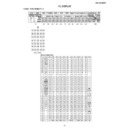
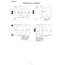
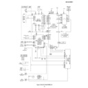
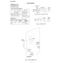
Figure 67-1 BLOCK DIAGRAM OF IC
Figure 67-2 BLOCK DIAGRAM OF IC
SD-EX100H
– 68 –
IC301 VHiLC75341M-1: Audio Processor (LC75341M)
1
DI
Serial data and clock input terminal for control.
2
CE
Chip enable terminal.
When changing from "H" to "L", data is written in the internal latch and each analog switch is turned on.
Data transmission is enabled at "H" level.
When changing from "H" to "L", data is written in the internal latch and each analog switch is turned on.
Data transmission is enabled at "H" level.
3
VSS
Ground terminal.
4
LOUT
Bass band filter construction capacitor/resistor connection terminal and bass/treble output terminal.
5
LBASS
Bass band filter capacitor and resistor connection terminal.
6
LTRE
Treble band filter capacitor connection terminal.
7
LIN
L-CH signal input terminal.
8
LSELO
Input selector output terminal.
9-12 (11*)
L4-L1
Input signal terminal.
13-16 (14*) R1-R4
Input signal terminal.
17
RSELO
Input selector output terminal.
18
RIN
R-CH signal input terminal.
19
RTRE
Treble band filter capacitor connection terminal.
20
RBASS
Bass band filter capacitor and resistor connection terminal.
21
ROUT
Bass band filter capacitor/resistor connection terminal and bass/treble output terminal.
22
Vref
0.5
×
VDD voltage generation section for analog ground. Connect a capacitor of 10
µ
F or more between
Vref and AVSS (VSS) as a countermeasure against the power supply ripple.
23
VDD
Power supply terminal.
24
CL
Serial data and clock input terminal for control.
Pin No.
Terminal Name
Function
In this unit, the terminal with asterisk mark (*) is (open) terminal which is not connected to the outside.
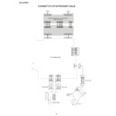
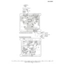
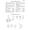
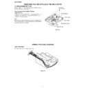
Figure 68 BLOCK DIAGRAM OF IC
4
5
6
7
8
9
10
11
12
13
14
15
16
17
18
19
20
21
22
23
24
1
2
3
LVref
RVref
CCB
INTERFACE
CONTROL
CIRCUIT
LOGIC
CIRCUIT
CONTROL
CIRCUIT
ROUT
RBASS
RTRE
RIN
RSELO
L1
L2
L3
L4
R1
R2
R3
R4
LOUT
LBASS
LTRE
LIN
LSELO
VSS
CE
DI
CL
VDD
Vref
24
23
22
21
20
19
18
17
16
15
14
13
1
2
3
4
5
6
7
8
9
10
11
12
LC75341M
CL
VDD
Vref
ROUT
RBASS
RTRE
RIN
RSELO
R4
R3
R2
R1
DI
CE
VSS
LOUT
LBASS
LTRE
LIN
LSELO
L4
L3
L2
L1
– 69 –
SD-EX100H
IC701 VHiTA2157F/-1: Head AMP. (TA2157F)
94k
Ω
22k
Ω
15pF
240k
Ω
94k
Ω
22k
Ω
40pF
40pF
180k
Ω
180k
Ω
60k
Ω
60k
Ω
3k
Ω
3k
Ω
20k
Ω
20k
Ω
20k
Ω
40k
Ω
40k
Ω
10pF
15pF
13
GVSW
18
RFRPIN
19
RFGO
RFGC
20
21
AGCIN
22
RFO
23
RFN
24
GND
12
RFDC
11
TEO
10
TEN
9
TEBC
8
SEL
7
LDO
6
MDI
5
TNI
4
TPI
3
FPI
2
FNI
1
VCC
20k
Ω
20k
Ω
15k
Ω
2k
Ω
1.75k
Ω
14k
Ω
1k
Ω
50k
Ω
2k
Ω
1.3V
20k
Ω
12k
Ω
12k
Ω
20k
Ω
40k
Ω
50k
Ω
15k
Ω
30k
Ω
20k
Ω
240k
Ω
10pF
14
VRO
15
FEO
16
FEN
17
RFRP
BOTTOM
PEAK
PEAK
x0.5
x2
K
x0.5
x2
1
50uA
40uA
1
VCC
—
3.3V power supply terminal
2
FNI
Input
Main beam amp input terminal
3
FPI
Input
Main beam amp input terminal
4
TPI
Input
Sub-beam amp input terminal
5
TNI
Input
Sub-beam amp input terminal
6
MDI
Input
Monitor photodiode amplifier input terminal
7
LDO
Output
Laser diode amp output terminal
8
SEL
Input
APC circuit ON/OFF signal, LDO terminal control input terminal and bottom/peak
detection frequency switching terminal
detection frequency switching terminal
9
TEBC
Input
Tracking error balance adjustment signal input terminal
• TEBC input voltage
• TEBC input voltage
10
TEN
Input
Tracking error signal generation amp antiphase input terminal
11
TEO
Output
Tracking error signal generation amp output terminal
12
RFDC
Output
RF signal peak detection output terminal
13
GVSW
Input
AGC, FE, TE amp gain switching terminal
14
VRO
Output
Reference voltage (VRO) output terminal • VCC=3.3V: VRO=1/2 VCC
15
FEO
Output
Focus error signal generation amp output terminal
16
FEN
Input
Focus error signal generation amp antiphase input terminal
17
RFRP
Output
Signal generation amp output terminal for track count
18
RFRPIN
Input
Signal generation amp input terminal for track count
19
RFGO
Output
RF signal amplitude adjustment amp output terminal
20
RFGC
Input
RF amplitude adjustment control signal input terminal • RFGC input voltage
21
AGCIN
Input
RF signal amplitude adjustment amp input terminal
22
RFO
Output
RF signal generation amp output terminal
23
RFN
Input
RF signal generation amp input terminal
24
GND
—
GND terminal
Terminal Name
Pin No.
Input/Output
Function
GND
OFF
Connection to VCC via 1k
Ω
Hi-z
ON
Control signal output
VCC
ON
Control signal output
SEL
APC circuit
LDO
GND
CD-RW
Hi-z
CD-DA
VCC
CD-CA
GVSW
Mode
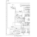
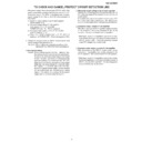
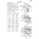
Figure 69 BLOCK DIAGRAM OF IC

