Sharp CD-E250 (serv.man18) Service Manual ▷ View online
CD-E250E
CD-E550E
– 50 –
44
RVSS
—
—
GND for Right channel. Must be connected to 0 V.
45
RCHO
Output
LVDD /2
Right channel output.
46
RVDD
Input
—
Power supply for Right channel.
47
XVDD
Input
—
Power supply for crystal oscillator.
48
XOUT
Output
Oscillator
Connected for the 33.8688 MHz crystal oscillator ciement.
49
XIN
Input
Oscillator
50
FSX/16MIN
Input/Output
Input
7.35 kHz Synchronization signal monitor port.
or Clock input port for Digital filter & D/A
or Clock input port for Digital filter & D/A
51
XVSS
—
—
Crystal
GND for crystal oscillator. Must be connected to 0 V.
Oscillator
52*
C2F
Output
H
C2 FLAG monitor port.
53*
EFLG
Output
L
C1, C2 error corrected monitor port.
54*
16MOUT
Output
Clock
16.9344 MHz output port.
55
ASLRCK
Input
—
Left/Right clock input port.
(If this port does not use, must be connect to 0 V.)
(If this port does not use, must be connect to 0 V.)
56
ASDACK
Input
—
Bit clock input port.
(If this port does not use, must be connect to 0 V.)
(If this port does not use, must be connect to 0 V.)
57
ASDFIN
Input
—
Left/Right channel data input port.
(If this port does not use, must be connect to 0 V.)
(If this port does not use, must be connect to 0 V.)
58*
LRCK
Output
L
Left/Right clock output port.
59*
BCK
Output
L
Digital data
Bit clock output port.
60*
DATA
Output
L
Left/Right channel data output port.
61
CE
Input
—
Chip enable signal input port.
62
CL
Input
—
Microcomputer
Data transfer clock input port.
63
DI
Input
—
Interface
Data input port.
64
DO
Output
(H)
Data output port. (N-ch. open drain output.)
65
*WRQ
Output
H
Interruption signal output.
66
*RES
Input
—
Chip reset signal input port.
This port must be set LOW after first applied power on.
This port must be set LOW after first applied power on.
67
DRF
Output
L
Focus detection output port.
68
VDD5
Input
—
Power supply for Microprocessor.
69
VSS
—
—
GND for digital circuit. Must be connected to 0 V.
70
CONT3
Input/Output
Input
General purpose port 3.
71
CONT2
Input/Output
Input
General purpose port 2.
72*
CONT1
Input/Output
Input
General purpose port 1.
73
PDO1
Output
—
Internal VCO control phase comparator output port 1.
74
PDO2
Output
Input
Internal VCO control phase comparator output port 2.
75
VVSS
—
—
GND for internal VCO. Must be connected to 0 V.
76
PCKIST
Input
—
PDO output current adjustment resistor connection port.
77
VVDD
Input
—
Power supply for internal VCO.
78
FR
Input
—
VCO frequency range adjustment port.
79
LDS
Input
—
LASER power detected signal input port.
80
LDD
Output
—
LASER power control signal output port.
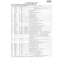
IC401 VHiLC78646E-1: Servo/Signal Control (LC78646E) (2/2)
Pin No.
Function
Terminal Name Input/Output Setting in Reset
Right channel
D/A converter
D/A converter
Anti-shock
Controlled with serial data command from micro-
computer. When not used, General purpose input/
output terminal. Set it as the input terminal and open
it by connecting to 0 V, or set it as the output terminal
and open it.
computer. When not used, General purpose input/
output terminal. Set it as the input terminal and open
it by connecting to 0 V, or set it as the output terminal
and open it.
In this unit, the terminal with asterisk mark (*) is (open) terminal which is not connected to the outside.
Be sure to supply the same potential to each power terminal. (VVDD, ADAVDD, VDD, LVDD, RVDD, XVDD)
Terminal witch is controlled by the power terminal (VDD5 V) for a microcomputer interface :
CE (61 pin), CL (62 pin), DI (63 pin), DO (64 pin), WRQ (65 pin), RES (66 pin), DRF (67 pin)
Terminal witch is controlled by the power terminal (VDD5 V) for a microcomputer interface :
CE (61 pin), CL (62 pin), DI (63 pin), DO (64 pin), WRQ (65 pin), RES (66 pin), DRF (67 pin)
Crystal
Oscillator
PLL
– 51 –
CD-E250E
CD-E550E
Figure 51 BLOCK DIAGRAM OF IC
IC401 VHiLC78646E-1: Servo/Signal Control (LC78646E)
1
2
3
4
5
6
7
8
9
10
11
12
13
14
15
16
17
18
19
20
21
22
23
24
25
26
27
28
29
30
31
32
33
34
35 36
37
38
39
40
80
79
78
77
76
75
74
73
72
71
70
69
68
67
66 65
64
63
62
61
60
59
58
57
56
55
54
53
52
51
50
49
48
47
46
45
44
43
42
41
SLCO
SLCIST
EFMIN
RF
RFVDD
RFVSS
FIN1
FIN2
TIN1
TIN2
VREF
REF1
FE
TEC
TE
RFMON
JITTC
ADAVDD
ADAVSS
TDO
FDO
SPDO
SLDO
GPDAC
CONT4
CONT5
SBCK/CONT6
SBCK/FG
DEFECT
V/*P
FSEQ
MONI1
MONI2
MONI3
MONI4
MONI5
(3.3V)VSS
VDD
DOUT
TEST
LDD
LDS
FR
VVDD
PCKIST
VVSS
PD02
PD01
CONT1
CONT2
CONT3
VSS
VDD5
DRF
*RES
*WRQ
DO
DI
CL
CE
DATA
DATACK
LRSY
ASDFIN
ASDACK
ASLRCK
16MOUT
EFLG
C2F
XVSS
FSX/16MIN
XIN
XOUT
XVDD
RVDD
RCHO
RVSS
LVSS
LCHO
LVDD
LC78646E
+
–
+
–
–
–
+
+
MIX
LPF
LPF
LPF
TBAL
TBAL
RAM
LEVEL SET
EQ
SW
PH
BH
+
–
+
–
+
–
+
–
MNI
CONT
A/D
SERVO PROCESSOR
TRACK JUMP
AUTO ADJUST
JITTER
DETECT
1bit DAC
8FS
DIGITAL FILTER
GENERAL-PURPOSE
PORTS
COMMAND
INTERFACE
CLOCK
GENERATOR
CLV,CAV
CONTROL
PLL
VCEC
SLICE LEVEL
CONTROL
APC
S/H
D/A
SW
DRF
RUPTURE DEFECT
FRAME SYNC
DETECT,PROTECT INSERT,
EFM DECODE
VDD5V
SUBCODE DECODE CRC
MONITOR SIGNAL SELECTOR
RAM
ERROR
CORRECTION
AUDIO CD
C1-2,C2-2
AUDIO OUT
SERIAL
OUT
EXTERNAL
AUDIO IN
INTERPOLATION
MUTE
ATTENUATION
DEEMPHSIS
LPF
FIN1
FIN2
TIN1
TIN2
REF1
DEFECT
ADIN
ADAVDD
ADAVSS
JITTC
SLCO
EFMIN
SLCIST
PCK
PDO1
PDO2
PDO2
FR
PCKIST
VVDD
VVSS
SBCK/FG
XIN
XOUT
16MOUT
XVDD
XVSS
*RES
*WRQ
CL
CE
DI
DO
VDD5V
CONT1, 2, 3
TEST
CONT4, 5,
SBCK/CONT6
LVDD
LVSS
LCHO
RCHO
RVDD
RVSS
ASDFIN
ASDACK
ASLRCK
DATA
DATACK
LRSY
DOUT
EFLG
C2F
FSX/16MIN
MONI1~5
VSS
VDD
V/*P
FSEQ
DRF
GPDAC
SPD0
SLD0
TD0
FD0
LDS
LDD
VREF
RFMON
RFVSS
RFVDD
RF
TEC
TE
FE
+
–
+
–
AGC
CD-E250E
CD-E550E
– 52 –
IC601 VHiLC75341M-1: Audio Processor (LC75341M)
Figure 52 BLOCK DIAGRAM OF IC
19
20
21
22
23
24
1
2
3
4
5
6
7
8
9
10
11
12
13
14
15
16
18
17
LVref
RVref
CONTROL
CIRCUIT
CONTROL
CIRCUIT
CONTROL
CIRCUIT
LOUT
LBASS
LIN
LSEL0
L4
L3
L2
L1
R1
R2
R3
R4
RSEL0
RIN
RTRE
LTRE
RBASS
ROUT
VREF
VDD
CLK
DI
CE
VSS
CCB
INTERFACE
CD
Tuner
Tape
Video
IC601 VHiLC75341M-1: Audio Processor (LC75341M)
Terminal Name
Pin No.
Function
1
DI
Serial data and clock input pin
for control.
for control.
2
CE
Chip enable pin.
Data written into an internal latch
in a timing of "H" to "L".
Each analog switch is activated.
Data transfer enabled at "H" level.
Data written into an internal latch
in a timing of "H" to "L".
Each analog switch is activated.
Data transfer enabled at "H" level.
3
VSS
Ground pin.
4
LOUT
Bass band filter comprising
capacitor and resistor connection
pin and bass/treble output pin.
capacitor and resistor connection
pin and bass/treble output pin.
5
LBASS
Bass band filter comprisingcapacitor
and resistor connection pin.
and resistor connection pin.
6
LTRE
Treble band filter comprising
capacitor and resistor connection
pin.
capacitor and resistor connection
pin.
7
LIN
Volume + equaliser output pin
8
LSEL0
Input selector output pin.
9-12
L4-1
Input signal pin.
Terminal Name
Pin No.
Function
13-16
R1-4
Input signal pin.
17
RSEL0
Input selector output pin.
18
RIN
Volume + equaliser output pin
19
RTRE
Treble band filter comprising
capacitor and resistor connection
pin.
capacitor and resistor connection
pin.
20
RBASS
Bass band filter comprisingcapacitor
and resistor connection pin.
and resistor connection pin.
21
ROUT
Bass band filter comprising
capacitor and resistor connection
pin and bass/treble output pin.
capacitor and resistor connection
pin and bass/treble output pin.
22
VREF
0.5x VDD voltage generation block
for analog ground. Capacitor of
several 10
for analog ground. Capacitor of
several 10
µ
F to be connected
between VREF and AWSS (VSS) as
a countermeasure against power
ripple.
a countermeasure against power
ripple.
23
VDD
Supply pin
24
CLK
Serial data and clock input pin
for control.
for control.
– 53 –
CD-E250E
CD-E550E
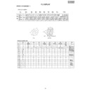
IC701 RH-iX0058SJZZ: System Microcomputer (IX0058SJ) (CD-E250E) (1/2)
IC701 RH-iX0065SJZZ: System Microcomputer (IX0065SJ) (CD-E550E) (1/2)
IC701 RH-iX0065SJZZ: System Microcomputer (IX0065SJ) (CD-E550E) (1/2)
In this unit, the terminal with asterisk mark (*) is (open) terminal which is not connected to the outside.
1
P16
TIMER_LED
Output
Timer LED control.
2*
P17
RDS_DATA
Input/Output
Open
3*
P30
RDS_CLE
Input/Output
Open
4
P31
CD_CE
Output
CD DSP CE output.
5
P32
CD_RES
Output
CD DSP reset.
6
P33
CD_DRF
Input
CD DRF level detection.
7
P34
CD_WRQ
Input
CD write read request.
8*
P35
PROG0
Input/Output
Open
9*
P36
PROG1
Input/Output
Open
10*
P37
PROG2
Input/Output
Open
11
RES
RESET IN PUT
Input
Reset signal input.
12
XT1
XT1
Input
Open
13
XT2
XT2
Input/Output
Open
14
VSS1
GND
–
Ground voltage.
15
CF1
CF1
Input
Main clock.
16
CF2
CF2
Output
Main clock.
17
VDD1
VDD1
–
(+) Power supply.
18
P80
KEY1_IN
Input
Key input.
19
P81
KEY2_IN
Input
Key input.
20*
P82
NO USE
Input/Output
Open
21
P83
FAN_PRT
Input
Fan protect circuit input.
22
P84
MODE_CKECK
Input
Ground level input.
23
P85
T2_TAPE2_SW
Input
Tape SW detection.
24*
P86
T1_TAPE1_SW
Input/Output
Open
25*
P87
RDS_VSM
Input/Output
Open
26
P70
SYS_STOP
Input
System stop input.
27
P71
X-BASS/DEMO
Input
Key input.
28
P72
POWER_KEY
Input
Key input.
29
P73
IRQ
Input
Remocon input.
30-38
S0/T0-S8/T8
G9-G1
Output
FL(VFD) segment driver.
39*-45*
S9/T9-S15/T15
NO USE
Input/Output
Open
46
VDD3
VDD3
–
(+) Power supply.
47-50
S16-S19
P1-P4
Output
FL(VFD) segment driver.
51
FIX0
GND
–
Connect to GND.
52-67
S20-S35
P5-P20
Output
FL(VFD) segment driver.
68
S36
DISC_NO_SW
Input
Tray disc no. SW detection.
69
S37
DISC1_SW
Input
Tray disc 1 SW detection.
70
S38
DISC_UP_SW
Input
Tray disc up SW detection.
71
S39
CLOSE_SW
Input
Tray close SW detection.
72
VDD4
VDD4
–
(+) Power supply.
73
S40
ROTATE
Output
Tray motor control.
74
S41
DISC_DOWN_SW
Input
Tray disc down SW detection.
75
S42
OPEN_SW
Input
Tray open SW detection.
76
S43
TAPE_BIAS
Output
Tape record bias.
77
S44
REC_PLAY
Output
Tape REC/PLAY change.
78
S45
REC
Input
Tape 2 rec SW detection.
79
S46
MOTOR
Output
Tape motor control.
80
S47
T1_SOL
Output
Tape 1 solenoid control.
81
S48
T2_SOL
Output
Tape 2 solenoid control.
82
S49
T1_RUN_PLUS
Input
Tape 1 RUN PULSE input.
83
S50
T2_RUN_PLUS
Input
Tape 2 RUN PULSE input.
Port Name
Terminal Name
Pin No.
Input/Output
Function
Display

