Sharp CD-C621H (serv.man12) Service Manual ▷ View online
– 43 –
CD-C621H
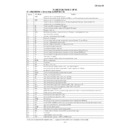
FUNCTION TABLE OF IC
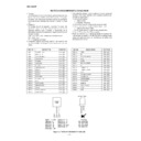
IC1 VHiLA9241M/-1: Servo Amp. (LA9241M) (1/2)
1
FIN2
Connection pin for photodiode of pickup.
RF signal is generated through addition with FIN pin, and FE signal is generated through subtraction.
RF signal is generated through addition with FIN pin, and FE signal is generated through subtraction.
2
FIN1
Connection pin for photodiode of pickup.
3
E
Connection pin for photodiode of pickup. TE signal is generated through subtraction with F pin.
4
F
Connection pin for photodiode of pickup.
5
TB
Pin for input of DC component of TE signal.
6
TE-
Pin to connect gain setting resistor of TE signal to TE signal.
7
TE
TE signal output pin.
8
TESI
TES (Track error sense) comparator input pin. TE signal is band-passed and input.
9
SCI
Input pin for shock detection.
10
TH
Pin to set time constant of tracking gain.
11*
TA
TA amplifier output pin.
12
TD-
Pin to compose tracking phase compensation constant between TD and VR pins.
13
TD
Pin to set tracking phase compensation.
14
JP
Pin to set amplitude of tracking jump signal (kick pulse).
15
TO
Tracking control signal output pin.
16
FD
Focusing control signal output pin.
17
FD-
Pin to compose focusing phase compensation constant between FD and FA pins.
18
FA
Pin to compose focusing phase compensation constant between FD-/FA-pins.
19
FA-
Pin to compose focusing phase compensation constant between FA and FE pins.
20
FE
Output pin of FE signal.
21
FE-
Pin to connect gain setting resistor of FE signal across TE pin.
22
AGND
GND for analog signal.
23
NC
No connect.
24
SPI
Spindle amplifier input.
25
SPG
Pin to connect gain setting resistor in the 12cm mode of spindle.
26
SP-
Pin to connect spindle phase compensation constant together with SPD pin.
27
SPD
Spindle control signal output pin.
28
SLEQ
Pin to connect thread phase compensation constant.
29
SLD
Thread control signal output pin.
30
SL-
Input pin of thread feed signal from micro computer.
31
SL+
Input pin of thread feed signal from micro computer.
32
JP-
Input pin of tracking jump signal from DSP.
33
JP+
Input pin of tracking jump signal from DSP.
34
TGL
Input pin of tracking gain control signal from DSP. TGL = Gain low at "H"
35
TOFF
Input pin of tracking off control signal from DSP. TOFF = Off at "H"
36
TES
Output pin of TES signal to DSP.
37
HFL
(HIGH FREQUENCY LEVEL) is used to judge whether main beam is positioned on the bit or on the mirror.
38
SLOF
Thread servo off control input pin.
39
CV-
Pin to input CLV error signal from DSP.
40
CV+
Pin to input CLV error signal from DSP.
41
RFSM
RF output pin.
42
RFS-
Pin to set gain of RF and set 3T compensation constant together with RFSM pin.
43
SLC
(SLICE LEVEL CONTROL) is the output pin to control of the level of the data slice with RF waveform DSP.
44
SLI
Input pin to control the level of data slice with DSP.
45
DGND
GND pin in the digital system.
46
FSC
Output pin for focus search smoothening capacitor.
47
TBC
(Tracking Balance Control) Pin to set EF balance variable range.
48*
NC
No connect.
49
DEF
Defect detection output pin of disk.
50
CLK
Reference clock input pin. 4.23MHz of DSP is input.
Pin No.
Port Name
Function
In this unit, the terminal with asterisk mark (*) is (open) terminal which is not connected to the outside.
CD-C621H
– 44 –
IC1 VHiLA9241M/-1:Servo Amp.(LA9241M) (2/2)
Pin No.
Port Name
Function
51
CL
Micro computer command clock input pin.
52
DAT
Micro computer command data input pin.
53
CE
Micro computer command chip enable input pin.
54
DRF
(DETECT RF) RF level detection output.
55
FSS
(Focus Serch Select) Pin to switch focus search mode. (
±
search/+ search for reference voltage)
56
VCC2
VCC pin for servo system and digital system.
57
REFI
Pin to connect pass control for reference voltage.
58
VR
Reference voltage output pin.
59
LF2
Pin to set defect detection time constant of disk.
60
PH1
Pin to connect capacitor for peak hold of RF signal.
61
BH1
Pin to connect capacitor for bottom hold of RF signal.
62
LDD
APC circuit output pin.
63
LDS
APC circuit output pin.
64
VCC1
RF system VCC pin.
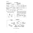
Figure 44 BLOCK DIAGRAM OF IC
1
FIN2
FIN1
E
F
TB
TE-
TE
TESI
SCI
TH
TA
TD-
TD
JP
TO
FD
FD-
FA
FA-
FE
FE- AGND SP
SPI
SPG
SP-
SPD
SLEQ
SLD
SL- SL+
JP-
JP+
TGL
TOFF
TES
HFL
SLOF
CV-
CV+
RFSM
RFS-
SLC
SLI
DGND
FSC
TBC
NC
DEF
CLK
CL
DAT
CE
DRF
FSS
VCC2
REFI
VR
LP2
PH1
BH1
LDD
LDS
SLC
RF AMP
TE
F.SERVO & F.LOGIC
SPINDLE SERVO
SLED SERVO
VCC1
2
3
4
6
7
5
8
9
10
11
12
13
14
15
16
17
18
19
20
21
23
22
25
26
27
28
29
30
31
32
33
34
35
36
37
38
39
40
41
42
43
44
46
47
48
49
50
51
52
53
54
55
56
57
58
59
61
60
62
63
64
45
24
APC
RF DET
REF
VCA
VCA
INTER FACE
BAL
µ
-COM
I/V
T.SERVO & T.LOGIC
NC
– 45 –
CD-C621H
1
DEFI
Input
Defect detection signal (DFF) input terminal. (When this terminal is not used, connect it to 0V.)
2
TAI
Input
For PLL Input terminal for test. Pull-down resistor built in. Be sure to connect this terminal to 0V.
3
PDO
Output
Phase comparison output terminal for external VCO control.
4
VVSS
—
Grounding terminal for built-in VCO. Be sure to connect this terminal to 0V.
5
ISET
Input
Resistor connection terminal for adjustment of PDO output current.
6
VVDD
—
Power terminal for built-in VCO.
7
FR
Input
For VCO frequency range adjustment.
8
VSS
—
Digital system grounding terminal. Be sure to connect this terminal to 0V.
9
EFMO
Output
For slice level control EFM signal output terminal.
10
EFMIN
Input
EFM signal input terminal.
11
TEST2
Input
Input terminal for test. Pull-down resistor built-in. Be sure to connect this terminal to 0V.
12
CLV+
Outout
Output for disc motor control. 3-value output is enabled according to command.
13
CLV-
Output
Output for disc motor control. 3-value output is enabled according to command.
14
V/P
Output
Rough servo/phase control automatic selection monitor output terminal.
"H": Rough servo, "L": Phase servo
"H": Rough servo, "L": Phase servo
15
HLF
Intput
Track detection signal input terminal. Schmidt input.
16
TES
Input
Tracking error signal input terminal. Schmidt input.
17
TOFF
Output
Tracking OFF output terminal.
18
TGL
Output
Output terminal for tracking gain selection. "L": Gain raising.
19
JP+
Output
Output for track jump control. 3-value output is enabled according to command.
20
JP-
Output
Output for track jump control. 3-value output is enabled according to command.
21*
PCK
Output
Clock monitor terminal for EFM data play-back. Phase lock: 4.3218 MHz.
22*
FSEQ
Output
Sync signal detection output terminal.
When the sync signal detected from the EFM signal coincides with the internally generated sync
signal: "H"
When the sync signal detected from the EFM signal coincides with the internally generated sync
signal: "H"
23
VDD
—
Digital system power terminal.
24
CONT1
Input/Output General-use input/output terminal 1.
25
CONT2
Input/Output General-use input/output terminal 2.
26
CONT3
Input/Output General-use input/output terminal 3.
27
CONT4
Input/Output General-use input/output terminal 4.
28*
CONT5
Input/Output General-use input/output terminal 5.
29*
EMPH/CONT6
Output
Deemphasis monitor terminal. "H": Deemphasis disc play-back. General-use output terminal 6.
30*
C2F
Output
C2 flag output terminal.
31*
DOUT
Output
Digital OUT output terminal. (EIAJ format)
32*
TEST3
Input
Input terminal for test. Pull-down resistor built-in. Be sure to connect this terminal to 0V.
33
TEST4
Input
Input terminal for test. Pull-down resistor built-in. Be sure to connect this terminal to 0V.
34
PCCL
Input
General-use input/output command recognition terminal. Pull-down resistor built in.
When this terminal is used for the same function as that of LC78622E, open or connect this
terminal to 0V.
H: Only the general-use input/output port command is controllable.
L: All command controls are enabled.
When this terminal is used for the same function as that of LC78622E, open or connect this
terminal to 0V.
H: Only the general-use input/output port command is controllable.
L: All command controls are enabled.
35*
MUTEL/CONT7
Output
L channel 1-bit DAC
Mute output terminal for L channel. General-use output terminal 7.
36
LVDD
—
Power terminal for L channel.
37
LCHO
Output
L channel output terminal.
38
LVSS
—
Grounding terminal for L channel. Be sure to connect this terminal to 0V.
39
RVSS
—
R channel 1-bit DAC
Grounding terminal for R channel. Be sure to connect this terminal to 0V.
40
RCHO
Output
R channel output terminal.
41
RVDD
—
Power terminal for R channel.
42*
MUTER/CONT8
Output
Mute output terminal for R channel. General-use output terminal 8.
43
XVDD
—
Power terminal for crystal oscillation.
44
XOUT
Output
16.9344 MHz crystal oscillator connection terminal.
45
XIN
Input
16.9344 MHz crystal oscillator connection terminal.
46
XVSS
—
Grounding terminal for crystal oscillation. Be sure to connect this terminal to 0V.
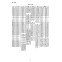
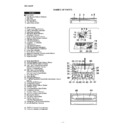
IC2 VHiLC78622N-1: Servo/Signal Control (LC78622NE) (1/2)
Pin
No.
No.
Function
Terminal Name Input/Output
Control with serial data command from microcomputer.
When this terminal is not used, set it as an input terminal
and connect to 0V or set it as an output terminal and
open.
When this terminal is not used, set it as an input terminal
and connect to 0V or set it as an output terminal and
open.
In this unit, the terminal with asterisk mark (*) is (open) terminal which is not connected to the outside.
CD-C621H
– 46 –
IC2 VHiLC78622N-1: Servo/Signal Control (LC78622NE) (2/2)
47*
SBSY
Output
Sub-code clock sync signal output terminal.
48*
EFLG
Output
C1, C2, single, double correction monitor terminal.
49*
PW
Output
Sub-code P, Q, R, S, T, U, and W output terminal.
50*
SFSY
Output
Sub-code frame sync signal output terminal. Falling occurs when the sub-code is in standby state.
51
SBCK
Input
Sub-code read clock input terminal. Schmidt input (When this terminal is not used, connect it to 0V.)
52*
FSX
Output
7.35 kHz sync signal (frequency-divided from crystal oscillation) output terminal.
53
WRQ
Output
Sub-code Q output standby output terminal.
54
RWC
Input
Read/Write control input terminal. Schmidt input.
55
SQOUT
Output
Sub-code Q output terminal.
56
COIN
Input
Command input terminal from microcomputer.
57
CQCK
Input
Command input taking-in clock or sub-code taking-out (from SQOUT) clock input terminal.
Schmidt input
Schmidt input
58
RES
Input
LSI resetting input terminal. When power is turned on, once "L" is set.
59*
TEST11
Output
Output terminal for test. Use this terminal in open state (usually "L" output).
60*
16M
Output
16.9344 MHz output terminal.
61
4.2M
Output
4.2336 MHz output terminal.
62
TEST5
Input
Input terminal for test. Pull-down resistor built-in. Be sure to connect this terminal to 0V.
63
CS
Input
Chip selection input terminal. Pull-down resistor built-in.
In noncontrol state connect this terminal to 0V.
In noncontrol state connect this terminal to 0V.
64
TEST1
Input
Input terminal for test. Pull-down resistor is not provided. Be sure to connect this terminal to 0V.
Note: The same potential must be supplied to the power terminals (VDD, VVDD, LVDD, RVDD, XVDD).
In this unit, the terminal with asterisk mark (*) is (open) terminal which is not connected to the outside.
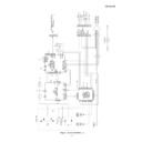
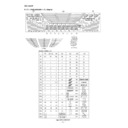
Figure 46 BLOCK DIAGRAM OF IC
Pin
No.
No.
Function
Terminal Name Input/Output
DEFI
EFMIN
FSEQ
V/P
PW
SBCK
SBSY
SFSY
CS
WRQ
SQOUT
COIN
RWC
CQCK
HFL
TES
TOFF
JP-
JP+
RES
TGL
CONT1
PCCL
CONT2
CONT3
CONT4
CONT5
EMPH/CONT6
EFLG
16M
4.2M
XVss
FSX
XIN
XOUT
XV
DD
RVss
RV
DD
MUTER/CONT7
RCHO
LCHO
MUTEL/CONT8
LVss
LV
DD
DOUT
C2F
EFMO
VV
DD
VVss
PDO
I SET
FR
PCK
TAI
TST11
TEST1
TEST2
TEST3
TEST4
TEST5
V
DD
Vss
CLV+
CLV-
Slice level
control
VCO colck oscillation
clock control
2 K x 8 b i t
R A M
RAM address
generator
Interpolation mute
Bilingual
Digital OUT
Digital
attenuator
X4 oversampling
digital filter
1 b i t D A C
L . P . F
XTAL system timing
generator
General-use port
Servo commander
µ
C O M
Interface
Subcode division
QCRC
C L V
Digital servo
Sync detection
EFM demodulation
Flag processing of C1/C2
error detection and correction
Display

