Sharp CD-C451H (serv.man14) Service Manual ▷ View online
– 57 –
CD-C451H
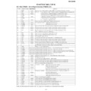
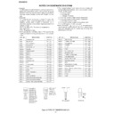
IC601 VHiLC75396N-1:Audio Processor (LC75396N)
1-3*
RF1C1-RF1C3
Terminal to connect capacitor of filter configuration for equalizer F1 band
Connect the capacitor between LF1C1(RF1C1) and LF1C2(RF1C2) between LF1C2 (RF1C2) and LF1C3(RF1C3).
Connect the capacitor between LF1C1(RF1C1) and LF1C2(RF1C2) between LF1C2 (RF1C2) and LF1C3(RF1C3).
4-6
RF2C1-RF2C3
Terminal to connect capacitor of filter configuration for equalizer F2 band
Connect the capacitor between LF2C1(RF2C1) and LF2C2(RF2C2) between LF2C2 (RF2C2) and LF2C3(RF2C3).
Connect the capacitor between LF2C1(RF2C1) and LF2C2(RF2C2) between LF2C2 (RF2C2) and LF2C3(RF2C3).
7-9
RF3C1-RF3C3
Terminal to connect capacitor of filter configuration for equalizer F3 band
Connect the capacitor between LF3C1(RF3C1) and LF3C2(RF3C2) between LF3C2 (RF3C2) and LF3C3(RF3C3).
Connect the capacitor between LF3C1(RF3C1) and LF3C2(RF3C2) between LF3C2 (RF3C2) and LF3C3(RF3C3).
10-12
RF4C1-RF4C3
Terminal to connect capacitor of filter configuration for equalizer F4 band
Connect the capacitor between LF4C1(RF4C1) and LF4C2(RF4C2) between LF4C2 (RF4C2) and LF4C3(RF4C3).
Connect the capacitor between LF4C1(RF4C1) and LF4C2(RF4C2) between LF4C2 (RF4C2) and LF4C3(RF4C3).
13
RF5
Terminal to connect capacitor of filter configuration for equalizer F5 band
Terminal to connect the externally provided capacitor
Terminal to connect the externally provided capacitor
14
RTOUT
Equalizer output terminal
15
RFIN
Input terminal of Rch front side 4dB step control
16
RFCOM
Common terminal of Rch front side 1dB step control
17
RFOUT
Output terminal of Rch front side control
18
RRIN
Input terminal of Rch rear side 4dB step control
19
RRCOM
Common terminal of Rch rear side 1dB step control
20
RROUT
Output terminal of Rch rear side control
21
RVREF
Internal analog ground terminal
22
VREF
Connect the capacitor of about several 10 uF between Vref and AVSS (VSS) so as to prevent power supply
ripple in the VDD/2 voltage generating section.
ripple in the VDD/2 voltage generating section.
23
CL
Terminal to input serial data and clock for control
24
DI
Terminal to input serial data and clock for control
25
CE
Chip enable terminal. Data is written in the internal latch with a timing of changing H to L, and the specific
analog switch is actuated. Data transfer is enabled on the H level.
analog switch is actuated. Data transfer is enabled on the H level.
26
VSS
GND
27
LVREF
Internal analog ground terminal
28
COUT
Output terminal of Lch rear side control
29
LRCOM
Common terminal of Lch rear side 1dB step control
30
CIN
Input terminal of Lch rear side 4dB step control
31
LFOUT
Output terminal of Lch front side control
32
LFCOM
Common terminal of Lch front side 1dB step control
33
LFIN
Input terminal of Lch front side 4dB step control
34
LTOUT
Equalizer output terminal
35
LF5
Terminal to connect capacitor of filter configuration for equalizer F5 band
Terminal to connect the externally provided capacitor
Terminal to connect the externally provided capacitor
36-38
LF4C3-LF4C1
Terminal to connect capacitor of filter configuration for equalizer F4 band
Connect the capacitor between LF4C1(RF4C1) and LF4C2(RF4C2) between LF4C2 (RF4C2) and LF4C3(RF4C3).
Connect the capacitor between LF4C1(RF4C1) and LF4C2(RF4C2) between LF4C2 (RF4C2) and LF4C3(RF4C3).
39-41
LF3C3-LF3C1
Terminal to connect capacitor of filter configuration for equalizer F3 band
Connect the capacitor between LF3C1(RF3C1) and LF3C2(RF3C2) between LF3C2 (RF3C2) and LF3C3(RF3C3).
Connect the capacitor between LF3C1(RF3C1) and LF3C2(RF3C2) between LF3C2 (RF3C2) and LF3C3(RF3C3).
42-44
LF2C3-LF2C1
Terminal to connect capacitor of filter configuration for equalizer F2 band
Connect the capacitor between LF2C1(RF2C1) and LF2C2(RF2C2) between LF2C2 (RF2C2) and LF2C3(RF2C3).
Connect the capacitor between LF2C1(RF2C1) and LF2C2(RF2C2) between LF2C2 (RF2C2) and LF2C3(RF2C3).
45-47*
LF1C3-LF1C1
Terminal to connect capacitor of filter configuration for equalizer F1 band
Connect the capacitor between LF1C1(RF1C1) and LF1C2(RF1C2) between LF1C2 (RF1C2) and LF1C3(RF1C3).
Connect the capacitor between LF1C1(RF1C1) and LF1C2(RF1C2) between LF1C2 (RF1C2) and LF1C3(RF1C3).
48
LTIN
Equalizer input terminal
49
LSELO
Input selector output terminal
50
LINVIN1
Operational amplifier reverse input terminal for input gain setting
51-55
L5-L1
Input signal terminal
56
VDD
Power terminal
57-61
R1-R5
Input signal terminal
62
RINVIN1
Operational amplifier reverse input terminal for input gain setting
63
RSELO
Input selector output terminal
64
RTIN
Equalizer input terminal
Pin No.
Function
Terminal Name
CD-C451H
– 58 –
1
VREF
Output
Reference voltage output (Vdda/2)
2
MPXIN
Input
Base band (multiplex) signal input
3
Vdda
—
4
Vssa
—
5
FLOUT
Output
Sub-carrier input (comparator input)
6
CIN
Input
Sub-carrier output (filter output)
7
T1
Input
Test input (to be always connected to ground)
8
T2
Input
Test input (standby control)
0: Normal operation/1: Standby state (crystal oscillation stop)
0: Normal operation/1: Standby state (crystal oscillation stop)
9*
T3 (RDCL)
Input/Output
Test I/O (RDS clock output)
10*
T4 (RDDA)
Input/Output
Test I/O (RDS data output)
11 *
T5 (RSFT)
Input/Output
Test I/O (Soft judgment control data output)
12
XOUT
Output
Crystal oscillation output
13
XIN
Input
Crystal oscillation input (external reference signal input)
14
Vddd
—
15
Vssd
—
16*
T6 (ERROR/57K/BE1)
Input/Output
Test I/O (Error existence/nonexistence output/playback carrier output/error block
number output)
number output)
17*
T7 (CORREC/ARI-ID/BE0
Input/Output
Test I/O (Error existence/nonexistence output/SK detection output/error block
number output)
number output)
18*
SYNC
Input/Output
Block sync detection output
19*
RDS-ID
Output
RDS detection output
20
DO
Output
Data output
21
CL
Input
Clock input
Serial data interface (CCB)
22
DI
Input
Data input
23
CE
Input
Chip enable
24
SYR
Input
Sync and RAM address reset (positive logic)
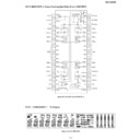
ICT21 VHiLC72720/-1:RDS Decorder (LC72720)
Terminal Name
Pin No.
Input/Output
Function
Figure 58 BLOCK DIAGRAM OF IC
Vdda
VREF
VREF
FLOUT CIN
Vssa
Vddd
Vssd
RDS-ID
SYNC
SYR
XOUT
XIN
MPXIN
DO
CL
DI
CE
CL
DI
CE
T1
T2
T3~T7
REFERENCE
VOLTAGE
57kHz
BPF
(SCF)
ANTIALIASING
FILTER
CCB
TEST
SMOOTHING
FILTER
RAM
(24 BLOCK DATA)
ERROR CORRECTION
(SOFT DECISION)
PLL
(57kHz)
CLOCK
RECOVERY
(1187.5Hz)
DATA
DECODER
SYNC
DETECT-1
OSC/DIVIDER
MEMORY CONTROL
CLK(4.332MHz)
SYNC
DETECT-2
SYNC/EC CONTROLLER
1
5
6
3
4
2
20
21
22
23
7
8
9,10,11
16,17
16,17
13
12
24
18
19
15
14
In this unit, the terminal with asterisk mark (*) is (open) terminal which is not connected to the outside.

