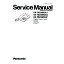
Panasonic KX-TS2350UAJ / KX-TS2350UAS / KX-TS2350UAT Service Manual ▷ View online
4
KX-TS2350UAJ/KX-TS2350UAS/KX-TS2350UAT
1 Safety Precautions
1.1.
For Service Technicians
• Repair service shall be provided in accordance with repair technology information such as service manual so as to pre-
vent fires, injury or electric shock, which can be caused by improper repair work.
1. When repair services are provided, neither the products nor their parts or members shall be remodeled.
2. If a lead wire assembly is supplied as a repair part, the lead wire assembly shall be replaced.
3. FASTON terminals shall be plugged straight in and unplugged straight out.
2. If a lead wire assembly is supplied as a repair part, the lead wire assembly shall be replaced.
3. FASTON terminals shall be plugged straight in and unplugged straight out.
• ICs and LSIs are vulnerable to static electricity.
When repairing, the following precautions will help prevent recurring malfunctions.
1. Cover plastic parts boxes with aluminum foil.
2. Ground the soldering irons.
3. Use a conductive mat on worktable.
4. Do not grasp IC or LSI pins with bare fingers.
2. Ground the soldering irons.
3. Use a conductive mat on worktable.
4. Do not grasp IC or LSI pins with bare fingers.
2 Warning
2.1.
About Lead Free Solder (Pbf: Pb free)
Note:
In the information below, Pb, the symbol for lead in the periodic table of elements, will refer to standard solder or solder that con-
tains lead.
We will use PbF solder when discussing the lead free solder used in our manufacturing process which is made from Tin (Sn),
Silver (Ag), and Copper (Cu).
This model, and others like it, manufactured using lead free solder will have PbF stamped on the PCB. For service and repair
work we suggest using the same type of solder.
Caution
• PbF solder has a melting point that is 50
°F ~ 70 °F (30 °C ~ 40 °C) higher than Pb solder. Please use a soldering iron with
temperature control and adjust it to 700
°F ± 20 °F (370 °C ± 10 °C).
• Exercise care while using higher temperature soldering irons.:
Do not heat the PCB for too long time in order to prevent solder splash or damage to the PCB.
• PbF solder will tend to splash if it is heated much higher than its melting point, approximately 1100
°F (600 °C).
• When applying PbF solder to double layered boards, please check the component side for excess which may flow onto the
opposite side (See the figure below).
5
KX-TS2350UAJ/KX-TS2350UAS/KX-TS2350UAT
2.1.1.
Suggested PbF Solder
There are several types of PbF solder available commercially. While this product is manufactured using Tin, Silver, and Copper
(Sn+Ag+Cu), you can also use Tin and Copper (Sn+Cu) or Tin, Zinc, and Bismuth (Sn+Zn+Bi). Please check the manufac
turer’s specific instructions for the melting points of their products and any precautions for using their product with other materi-
als. The following lead free (PbF) solder wire sizes are recommended for service of this product: 0.3 mm, 0.6 mm and 1.0 mm.
2.2.
Discarding of P. C. Board
When discarding P. C. Board, delete all personal information such as telephone directory and caller list or scrap P. C. Board.
3 Specifications
Note:
• Specifications are subject to change without notice.
6
KX-TS2350UAJ/KX-TS2350UAS/KX-TS2350UAT
4 Technical Descriptions
4.1.
Block Diagram
MELODY
SEQUENCER
LINE ADAPTATION
POWER EXTRACTION
DC MASK
CONTROL
LOGIC
TONE
GENERATOR
RING
FREQUENCY
DISCRIMINATION
OSC
RAM
MUTE
DIALLER
LINE
CURRENT
SENSE
SOFT CLIP
AGC
V
DD
LI
CI
LS
RI
STB
A
GND
LED
V
DD
V
SS
MO
FCI
HS/DP
LLC
OSC
MFL
M
ODE
C1
C2
C3
C4
R1
R2
R3
R4
M2
M1
RO
CS
IC1
KEY
PAD
R9
sv1
AGND
3.58
ADL
RS
R
T
Q1
Q2
D23
R55
R103
S3
L
H
OFF
D24
R14
IC2
R2
C1
Q8
Q3
Ringer
D2
C34
D17
C22
HS Speake
r
HS MIC
R10
C5
C9
R5
R6
KX-TS2350 BLOCK DIAGRAM
R102
58
1
2
7
KX-TS2350UAJ/KX-TS2350UAS/KX-TS2350UAT
4.2.
Circuit Operation
4.2.1.
Telephone Line Interface and Pulse Dial Circuit
When the hook switch SW1 is ON (off-hook), the circuit is closed, and current is supplied to the base of Q2 via the diode bridge
D17 and Q2 is On
D17 and Q2 is On
→ Q1 is ON (OFF-HOOK condition).
Q1 and Q2 are the dial pulse generating circuits, and are driven by the DIALER (IC1), when the DIALER Pin 10 of IC1 is LOW
→ Q2 is OFF and Q1 is OFF (break). If port Pin 10 is HIGH → Q2 is ON → Q1 is ON (make).
→ Q2 is OFF and Q1 is OFF (break). If port Pin 10 is HIGH → Q2 is ON → Q1 is ON (make).
4.2.2.
Tone Dial Circuit
Function:
The tone dialing circuit consists of a DTMF (Dual Tone Multi Frequency) signal generator (outputted from Pin 25 of the IC1) for
tone dialing, and also a circuit for outputting the signal to line.
The DTMF circuit identifies inputs from the 12 keys (1, 2, 3, 4, 5, 6, 7, 8, 9, 0, and #) by means of a total of seven frequencies,
that is four low frequencies (Low group) and three high frequencies (High group).
tone dialing, and also a circuit for outputting the signal to line.
The DTMF circuit identifies inputs from the 12 keys (1, 2, 3, 4, 5, 6, 7, 8, 9, 0, and #) by means of a total of seven frequencies,
that is four low frequencies (Low group) and three high frequencies (High group).
Circuit Description:
When a dial key is pressed, a DTMF signal is output from Pin 25 of IC1 as an analog synthetic wave.
The signal flow to the line is as follows.
Pin 25 of IC1
The signal flow to the line is as follows.
Pin 25 of IC1
→ Q3 → R9 → Q1 → Tel Line.
The DTMF signal is sent to the line via the following path. Q3 is an amplifier which is used to output the signal to line.
Shown below is the signal flow used to output the DTMF signal from the handset as a monitor tone when a dial key is pressed.
Pin 3 of IC1
Shown below is the signal flow used to output the DTMF signal from the handset as a monitor tone when a dial key is pressed.
Pin 3 of IC1
→ VR1 → C15 → Handset Speaker.
The signal combination and frequency corresponding to each dial key is shown on the next page.

