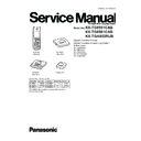
Panasonic KX-TG8551CAB / KX-TG8561CAB / KX-TGA855RUB Service Manual ▷ View online
7
KX-TG8551CAB/KXTG8561CAB/KX-TGA855RUB
3 Specifications
*1 KX-TG8551
*2 KX-TG8561
*2 KX-TG8561
Note:
• Design and specifications are subject to change without notice.
Note for Service:
• Operation range: Up to 300 m outdoors, Up to 50 m indoors, depending on the condition.
• Analog telephone connection: Telephone Line
• DECT repeater: KX-A405
• Optional headset: KX-TCA94EX
• Analog telephone connection: Telephone Line
• DECT repeater: KX-A405
• Optional headset: KX-TCA94EX
Standard:
DECT (Digital Enhanced Cordless Telecommunications), GAP (Generic Access Profile)
Number of Channels:
120 Duplex Channels
Frequency Range:
1.88 GHz to 1.90 GHz
Duplex Procedure:
TDMA (Time Division Multiple Access)
Channel Spacing:
1,728 kHz
Bit Rate:
1,152 kbit/s
Modulation:
GFSK (Gaussian Frequency Shift Keying)
RF Transmission Power:
Approx. 10mW (average power per channel)
Voice Coding:
ADPCM 32 kbit/s
Operating conditions:
0
°C - 40°C, 20 % - 80 % RH (Relative Humidity)
Power source (AC Adaptor):
220 - 240 V AC, 50/60 Hz
Base unit: PNLV226CE0Z
Charger: PNLV226CE0Z
Base unit: PNLV226CE0Z
Charger: PNLV226CE0Z
Power consumption:
Base unit
*1
:
Standby: Approx. 0.38 W
Maximum: Approx. 2.4 W
Base unit
Maximum: Approx. 2.4 W
Base unit
*2
:
Standby: Approx. 0.48 W
Maximum: Approx. 2.5 W
Charger:
Standby: Approx. 0.1 W
Maximum: Approx. 1.8 W
Maximum: Approx. 2.5 W
Charger:
Standby: Approx. 0.1 W
Maximum: Approx. 1.8 W
Dimensions:
Base unit
*1
: Approx. 103 mm x 106 mm x 43 mm
Base unit
*2
: Approx. 112 mm x 121 mm x 43 mm
Handset: Approx. 48 mm x 25 mm x 150 mm
Charger unit: Approx. 72 mm x 76 mm x 43 mm
Charger unit: Approx. 72 mm x 76 mm x 43 mm
Mass (Weight):
Base unit
*1
: Approx. 120 g
Base unit
*2
: Approx. 170 g
Handset: Approx. 110 g
Charger: Approx. 50 g
Charger: Approx. 50 g
8
KX-TG8551CAB/KXTG8561CAB/KX-TGA855RUB
4 Technical Descriptions
4.1.
Block Diagram (Base Unit)
Analog
Front
End
To TEL_LINE
Bridge
Rect D101
Hook Switch
Q141, Q142, Q161
Audio
Bell/Caller ID
Interface
CPU
MICn
LSRp
RINGn
CIDINp
CIDINn
CIDOUT
RINGOUT
BELL
HOOK
CHARGE_DET
Off-Hook Line Voltage
P
ARADET
A/D
D/A
ADPCM
Codec Filter
DSP
Speech Encoding
Speech Decoding
BMC
Burst Encoding
Burst Decoding
RF
PLL
XT
AL2
XT
AL1
EEPROM
SCL
SDA
To AC Adaptor
To HANDSET
Limit
Re
s
is
tor
R
3
71, R
3
72,
D
3
62
Charge
Detector
Power Failer Mode
Power Supply SW
Q351,IC351
CHARGE(+)
CHARGE(-)
Optional
for KX-TG8561 only
Optional
DC/DC con
v
e
rt
o
D
C
/D
C
c
o
n
v
e
rt
o
r
IC
3
02,L
3
01,
IC
3
0
2
,L
3
0
1
,
C
3
42,Q
3
10
C
3
4
2
,Q
3
1
0
Q
3
02
Q
Q
3
0
2
Q
3
01
Q
Q
3
0
1
2.4V
Reg.
1.8V
Reg.
2.85 V
2.4 V
1.8 V
BBIC
IC611
IC501
KX-TG8551/TG8561 BLOCK DIA
GRAM (BASE UNIT)
MOD/DEMOD
Charge
Pump
DCDC
Converter
Re
s
et
CP_VO
YT2
XTAL
X501X
5
0
1
10.368
MHz
RX
n
RX
p
TX
p
TX
n
TX
on
RX
on
D801
ANT1
ANT2
ANT1
ANT2
ANT1
ANT2
L1
L2
DCP
DCM
FLASH MEMORY
IC601
QSPI
FLASH MEMORY
IC502
CP_VO
YT1
3.0V
3.0V
RSTN
pin 62:
TG855x
pin 77:
TG856x
TAM-CSn
SPI-DI
SPI-DO
SPI-DO
SPICLK
QSPI-CS
DC-SENSE
DC-CTRL
QSPI-SCK
QSPI-IO 0-3
Q701, Q702
CD_I
QSPI
Control
9
KX-TG8551CAB/KXTG8561CAB/KX-TGA855RUB
4.2.
Circuit Operation (Base Unit)
4.2.1.
Outline
Base Unit consists of the following ICs as shown in Block Diagram (Base Unit) (P.8).
• DECT BBIC (Base Band IC): IC501
- Handling all the audio, signal and data processing needed in a DECT base unit
- Controlling the DECT specific physical layer and radio section (Burst Module Controller section)
- ADPCM code filter for speech encoding and speech decoding (DSP section)
- Echo-cancellation and Echo-suppression (DSP section)
- Any tones (tone, sidetone, ringing tone, etc.) generation (DSP section)
- DTMF receiver (DSP section)
- Clock Generation for RF Module
- ADC, DAC, timer, and power control circuitry
- PLL Oscillator
- Detector
- Compress/Expander
- First Mixer
- All interfaces (ex: QSPI FLASH MEMORY, EEPROM, LED, Analog Front End, etc.)
- DCDC Converter
- Integrated 1.9GHz PA for DECT
• EEPROM: IC611
- Temporary operating parameters (for RF, etc.)
• FLASH MEMORY: IC601 (for KX-TG8561 only)
- Voice Prompt (TAM) D/L Area
- ICM/OGM Recording Area
- ICM/OGM Recording Area
• Additionally,
- Power Supply Circuit (+3.0 V, +2.4 V, +1.8 V output)
- Crystal Circuit (10.368 MHz)
- Charge Circuit
- Telephone Line Interface Circuit
- Crystal Circuit (10.368 MHz)
- Charge Circuit
- Telephone Line Interface Circuit
• QSPI FLASH MEMORY IC502
- Main Program D/L Area
10
KX-TG8551CAB/KXTG8561CAB/KX-TGA855RUB
4.3.
Block Diagram (Base Unit RF Part)
KX-TG8551/8561 BLOCK DIAGRAM (Base Unit_RF Part)
DA801
ANT2
ANT1
TXON
RXON
RXp
RXn
ANT2
ANT1
TXp
TXn
Click on the first or last page to see other KX-TG8551CAB / KX-TG8561CAB / KX-TGA855RUB service manuals if exist.

