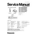
Panasonic KX-TCD235RUS / KX-TCD235RUT / KX-TCA121RUS / KX-TCA121RUT Service Manual ▷ View online
KX-TCD235RUS
KX-TCD235RUT
KX-TCA121RUS
KX-TCA121RUT
KX-TCD235RUT
KX-TCA121RUS
KX-TCA121RUT
Digital Cordless Phone
Silver Version
Titanium Black Version
(for Russia)
Telephone Equipment
ORDER NO. KM40507805CE
1
ABOUT LEAD FREE SOLDER (PbF: Pb free)
4
1.1.
Suggested PbF Solder
4
1.2.
How to recognize that Pb Free solder is used
5
2
FOR SERVICE TECHNICIANS
6
3
CAUTION
6
4
OPERATING INSTRUCTIONS
7
4.1.
Battery
7
4.2.
Location of Controls
9
4.3.
Connections
10
4.4.
Guide to Settings
11
4.5.
For Service Hint
12
5
DISASSEMBLY INSTRUCTIONS
13
5.1.
Base Unit
13
5.2.
Handset
14
5.3.
Charger Unit
15
6
HOW TO REPLACE THE HANDSET LCD
16
7
TROUBLESHOOTING FLOWCHART
17
7.1.
Check Power
18
7.2.
Check Battery Charge
19
7.3.
Check Link
20
7.4.
Check Handset Transmission
24
7.5.
Check Handset Reception
24
7.6.
Check Caller ID
24
7.7.
Check Base Speakerphone Transmission
24
7.8.
Check Base Speakerphone Reception
24
7.9.
Bell Reception
25
8
TROUBLESHOOTING BY SYMPTOM (BASE UNIT AND
CHARGER UNIT)
26
8.1.
Check Point (Base Unit)
26
8.2.
The Setting Method of JIG (Base Unit)
31
8.3.
Adjustment Standard (Base Unit)
32
8.4.
Check Point (Charger Unit)
33
8.5.
Adjustment Standard (Charger Unit)
33
9
TROUBLESHOOTING BY SYMPTOM (HANDSET)
34
9.1.
Check Point (Handset)
34
9.2.
Troubleshooting for Speakerphone (Handset)
37
9.3.
The Setting Method of JIG (Handset)
38
9.4.
Adjustment Standard (Handset)
39
10 THINGS TO DO AFTER REPLACING IC
40
10.1. Base Unit
40
10.2. Handset
40
11 RF SPECIFICATION
41
11.1. Base Unit
41
11.2. Handset
41
12 HOW TO CHECK THE SPEAKER OR RECEIVER
42
13 FREQUENCY TABLE (MHz)
42
14 BLOCK DIAGRAM (BASE UNIT)
43
15 CIRCUIT OPERATION (BASE UNIT)
44
15.1. Outline
44
15.2. Power Supply Circuit
45
15.3. Telephone Line Interface
46
15.4. Transmitter/Receiver
46
15.5. Pulse Dialling
46
16 BLOCK DIAGRAM (HANDSET)
47
17 CIRCUIT OPERATION (HANDSET)
48
17.1. Outline
48
17.2. Power Supply Circuit/Reset Circuit
48
17.3. Charge Circuit
48
17.4. Battery Low/Power Down Detector
48
17.5. Speakerphone
48
18 CIRCUIT OPERATION (CHARGER UNIT)
49
18.1. Power Supply Circuit
49
19 SIGNAL ROUTE
50
20 CPU DATA (BASE UNIT)
52
20.1. IC4 (BBIC)
52
21 CPU DATA (HANDSET)
55
21.1. IC1 (BBIC)
55
22 ENGINEERING MODE
57
22.1. Base Unit
57
22.2. Handset
60
23 EEPROM LAYOUT (BASE UNIT)
62
23.1. Scope
62
23.2. Introduction
62
23.3. EEPROM Layout
62
Note:
Because CONTENTS 4 is the extract from the Operating Instructions of this model, it is subject to change without notice. You can
download and refer to the original Operating Instructions on TSN Server for further information.
download and refer to the original Operating Instructions on TSN Server for further information.
CONTENTS
Page
Page
2
KX-TCD235RUS / KX-TCD235R UT / KX-TCA121RUS / KX-TCA121RUT
24 EEPROM LAYOUT (HANDSET)
67
24.1. Scope
67
24.2. Introduction
67
24.3. EEPROM contents
67
25 HOW TO REPLACE THE FLAT PACKAGE IC
70
25.1. PREPARATION
70
25.2. FLAT PACKAGE IC REMOVAL PROCEDURE
70
25.3. FLAT PACKAGE IC INSTALLATION PROCEDURE
71
25.4. BRIDGE MODIFICATION PROCEDURE
71
26 CABINET AND ELECTRICAL PARTS (BASE UNIT)
72
27 CABINET AND ELECTRICAL PARTS (HANDSET)
73
28 CABINET AND ELECTRICAL PARTS (CHARGER UNIT)
74
29 ACCESSORIES AND PACKING MATERIALS
75
29.1. KX-TCD235RUS/RUT
75
29.2. KX-TCA121RUS/RUT
76
30 TERMINAL GUIDE OF THE ICs, TRANSISTORS AND DIODES
77
30.1. Base Unit
77
30.2. Handset
77
30.3. Charger Unit
77
31 REPLACEMENT PARTS LIST
78
31.1. Base Unit
78
31.2. Handset
81
31.3. Charger Unit
82
31.4. Accessories and Packing Materials
83
31.5. Fixtures and Tools
83
32 FOR SCHEMATIC DIAGRAM
85
32.1. Base Unit (SCHEMATIC DIAGRAM (BASE UNIT_MAIN))
85
32.2. Handset (SCHEMATIC DIAGRAM (HANDSET))
85
32.3. Charger Unit (SCHEMATIC DIAGRAM (CHARGER UNIT))
85
33 SCHEMATIC DIAGRAM (BASE UNIT_MAIN)
86
34 SCHEMATIC DIAGRAM (BASE UNIT_OPERATION)
88
35 SCHEMATIC DIAGRAM (HANDSET)
90
36 SCHEMATIC DIAGRAM (CHARGER UNIT)
92
37 CIRCUIT BOARD (BASE UNIT_MAIN)
93
37.1. Component View
93
37.2. Flow Solder Side View
94
38 CIRCUIT BOARD (BASE UNIT_OPERATION)
95
38.1. Component View
95
38.2. Flow Solder Side View
96
39 CIRCUIT BOARD (HANDSET)
97
39.1. Component View
97
39.2. Flow Solder Side View
98
40 CIRCUIT BOARD (CHARGER UNIT)
99
40.1. Component View
99
40.2. Flow Solder Side View
99
3
KX-TCD235RUS / KX-TCD235R UT / KX-TCA121RUS / KX-TCA121RUT
1 ABOUT LEAD FREE SOLDER (PbF: Pb free)
Note:
In the information below, Pb, the symbol for lead in the periodic table of elements, will refer to standard solder or solder that
contains lead.
contains lead.
We will use PbF solder when discussing the lead free solder used in our manufacturing process which is made from Tin (Sn),
Silver (Ag), and Copper (Cu).
Silver (Ag), and Copper (Cu).
This model, and others like it, manufactured using lead free solder will have PbF stamped on the PCB. For service and repair
work we suggest using the same type of solder although, with some precautions, standard Pb solder can also be used.
work we suggest using the same type of solder although, with some precautions, standard Pb solder can also be used.
Caution
•
•
•
•
PbF solder has a melting point that is 50°F ~ 70°F (30°C ~ 40°C) higher than Pb solder. Please use a soldering iron with
temperature control and adjust it to 700°F ± 20°F (370°C ± 10°C). In case of using high temperature soldering iron, please
be careful not to heat too long.
temperature control and adjust it to 700°F ± 20°F (370°C ± 10°C). In case of using high temperature soldering iron, please
be careful not to heat too long.
•
•
•
•
PbF solder will tend to splash if it is heated much higher than its melting point, approximately 1100°F (600°C).
•
•
•
•
If you must use Pb solder on a PCB manufactured using PbF solder, remove as much of the original PbF solder as possible
and be sure that any remaining is melted prior to applying the Pb solder.
and be sure that any remaining is melted prior to applying the Pb solder.
•
•
•
•
When applying PbF solder to double layered boards, please check the component side for excess which may flow onto the
opposite side (See the figure below).
opposite side (See the figure below).
1.1. Suggested PbF Solder
There are several types of PbF solder available commercially. While this product is manufactured using Tin, Silver, and Copper
(Sn+Ag+Cu), you can also use Tin and Copper (Sn+Cu) or Tin, Zinc, and Bismuth (Sn+Zn+Bi). Please check the
manufacturer’s specific instructions for the melting points of their products and any precautions for using their product with other
materials.
(Sn+Ag+Cu), you can also use Tin and Copper (Sn+Cu) or Tin, Zinc, and Bismuth (Sn+Zn+Bi). Please check the
manufacturer’s specific instructions for the melting points of their products and any precautions for using their product with other
materials.
The following lead free (PbF) solder wire sizes are recommended for service of this product: 0.3mm, 0.6mm and 1.0mm.
4
KX-TCD235RUS / KX-TCD235R UT / KX-TCA121RUS / KX-TCA121RUT


