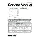
Panasonic KX-TDE100RU (serv.man2) Service Manual / Supplement ▷ View online
ORDER NO. KMS0710080SE
Pure IP-PBX
Model No.
KX-TDE100RU
(for Russia)
Please file and use this supplement manual together with the service manual for Model No. KX-TDE100RU
Order No. KMS0709411CE.
Order No. KMS0709411CE.
2
KX-TDE100RU
1 CHANGES
1.1.
REPLACEMENT PARTS LIST
Reason for Change
*The following items (1-8) indicate the reason for change. See the “Notes” column for each part in ORIGINAL AND NEW PARTS COMPARISON
LISTS.
1. Improve performance
2. Change of material or dimension
3. To meet approved specification
4. Standardization
5. Addition
6. Deletion
7. Correction
8. Other
*The following items (1-8) indicate the reason for change. See the “Notes” column for each part in ORIGINAL AND NEW PARTS COMPARISON
LISTS.
1. Improve performance
2. Change of material or dimension
3. To meet approved specification
4. Standardization
5. Addition
6. Deletion
7. Correction
8. Other
Interchangeability Code (Symbol:B) Following V-Z interchange abilities are indicated on the Notes in the bottom column.
Parts
Set Production
V Original
New
Early (before change)
Late (after change)
Late (after change)
Original or new parts may be used in early or late production sets.
Use original parts until exhausted, then stock new parts.
Use original parts until exhausted, then stock new parts.
W Original
New
Early (before change)
Late (after change)
Late (after change)
Original parts may be used in early production sets only. New parts may be used in early or
late production sets. Use original parts where possible, then stock new parts.
late production sets. Use original parts where possible, then stock new parts.
X Original
New
Early (before change)
Late (after change)
Late (after change)
New parts only may be used in early or late production sets.
Stock new parts.
Stock new parts.
Y Original
New
Early (before change)
Late (after change)
Late (after change)
Original parts may be used in early production sets only. New parts may be used in late
production sets only. Stock both original and new parts.
production sets only. Stock both original and new parts.
Z Other
Ref. No.
Part No.
Part Name & Description
Pcs
Remarks
Notes
Time of change
(Suffix)
Original (Old)
New
MAIN BOARD PARTS
IC101
IC101
C2DBYY000111
C2DBYY000380
IC
1
8
X
3
KX-TDE100RU
1.2.
IC101
Change from the Original Service Manual Section 16.1.1.
Pin No.
Pin Name
I/O
Function
A1
VSSQ-DDR
-
DDR I/O GND
A2
VCCQ-DDR
-
DDR I/O VCC
A3
DDR-VREF
I
DDR VREF
A4
MCLK
O
DDR clock
A5
MCLK#
O
DDR clock
A6
MWE#
O
DDR write enable
A7
MRAS#
O
DDR RAS
A8
BA0
O
DDR bank address 0
A9
MA10
O
DDR address
A10
MA1
O
DDR address
A11
MA3
O
DDR address
A12
PRESET#
I
Power on reset
A13
DRAK1#/MODE7
O/I
DMA channel 1 transfer request acknowledge/mode control 7
A14
DREQ0#
I
DMA channel 0 request
A15
DREQ3#/INTC#/
AUDATA1
AUDATA1
I/I/O
DMA channel 3 request/PCI interrupt C/H-UDI emulator
A16
DACK2#/MRE-
SETOUT#/AUDATA2
SETOUT#/AUDATA2
O/O/O DMA channel 2 bus acknowledgment/manual reset output/H-UDI emulator
A17
TDI
I
H-UDI data
A18
AUDSYNC/FCE#
O/O
H-UDI emulator/NAND flash CE
A19
AUDATA1/FD1
O/IO
H-UDI emulator/NAND flash data
A20
SIOF_SYNC/
HAC_SYNC/SSI_WS
HAC_SYNC/SSI_WS
IO/O/IO SIOF flame synchronous/HAC flame synchronous/SSI word select
A21
SCIF1_TXD/MCCLK/
MODE5
MODE5
O/O/I
SCIF 1 transmit data/card clock output/mode control 5
A22
XTAL2
O
RTC clock
A23
EXTAL2
I
RTC crystal resonator
4
KX-TDE100RU
A24
VDD-RTC
-
RTC VDD
A25
VSS-RTC
-
RTC GND
B1
VSSQ-DDR
-
DDR I/O GND
B2
VCCQ-DDR
-
DDR I/O VCC
B3
BKPRST#
I
Back-up reset
B4
CKE
O
DDR clock enable
B5
MA13
O
DDR address
B6
MCAS#
O
DDR CAS
B7
MCS#
O
DDR chip select
B8
BA1
O
DDR bank address 1
B9
MA0
O
DDR address
B10
MA2
O
DDR address
B11
MA4
O
DDR address
B12
VSS
-
Internal GND
B13
DRAK2#/CE2A#/
AUDCK
AUDCK
O/O/O DMA channel 2 transfer request acknowledge/PCMCIA CE2/H-UDI emulator
B14
DREQ1#
I
DMA channel 1 request
B15
DACK0#/MODE0
O/I
DMA channel 0 bus acknowledgement/mode control 0
B16
DACK3#/IRQOUT#/
AUDATA3
AUDATA3
O/O/O DMA channel 3 bus acknowledgement/interrupt request output/H-UDI emulator
B17
TDO
O
H-UDI data
B18
AUDCK/FALE
O/O
H-UDI emulator/NAND flash ALE
B19
AUDATA0/FD0
O/IO
H-UDI emulator/NAND flash data
B20
SIOF_RXD/
HAC_SDIN/SSI_SCK
HAC_SDIN/SSI_SCK
I/I/IO
SIOF receive data/HAC serial data incoming to Rx frame/SSI serial bit clock
B21
SCIF1_SCK/MCCMD
IO/IO
SCIF1 serial clock/MMCIF command response
B22
SCIF0_RXD/
HSPI_RX/FRB
HSPI_RX/FRB
I/I/I
SCIF receive data/HSPI receive data input/NAND flash ready or busy
B23
TCLK/IOIS16#
IO/I
TMU clock/PCMCIA IOIS16
B24
XRTCSTBI#
I
RTC standby
B25
VSSQ
-
I/O GND
C1
MDA0
IO
DDR data
C2
VCCQ-DDR
-
DDR I/O VCC
C3
VSSQ-DDR
-
DDR I/O GND
C4
VCCQ-DDR
-
DDR I/O VCC
C5
MA12
O
DDR address
C6
MA11
O
DDR address
C7
MA9
O
DDR address
C8
MA8
O
DDR address
C9
MA7
O
DDR address
C10
MA6
O
DDR address
C11
MA5
O
DDR address
C12
DRAK0#/MODE2
O/I
DMA channel 0 transfer request acknowledge/mode control 2
C13
DRAK3#/CE2B#/
AUDSYNC
AUDSYNC
O/O/O DMA channel 3 request acknowledgment/PCMCIA CE2/H-UDI emulator
C14
DREQ2#/INTB#/
AUDATA0
AUDATA0
I/I/O
DMA channel 2 request/PCI interrupt B/H-UDI emulator
C15
DACK1#/MODE1
O/I
DMA channel 1 bus acknowledgement/mode control 1
C16
TCK
I
H-UDI clock
C17
ASEBRK#/BRKACK
I
H-UDI emulator
C18
AUDATA3/FD3
O/IO
H-UDI emulator/NAND flash data
C19
SIOF_SCK/
HAC_BITCLK/
SSI_CLK
HAC_BITCLK/
SSI_CLK
IO/I/IO SIOF serial clock/HAC/SSI serial bit clock
C20
SIOF_TXD/
HAC_SDOUT/
SSI_SDATA
HAC_SDOUT/
SSI_SDATA
O/O/IO SIOF transmit data/HAC serial data/SSI serial data
C21
SCIF0_RTS#/
HSPI_CS#/FSE#
HSPI_CS#/FSE#
IO/IO/O SCIF modem control/HSPI chip selection/NAND flash spare area enable
C22
SCIF0_TXD/HSPI_TX/
FWE#/MODE8
FWE#/MODE8
O/O/O/I SCIF0 transmit data/HSPI transmit data/NAND flash write enable/mode control
8
C23
SCIF0_SCK/
HSPI_CLK/FRE#
HSPI_CLK/FRE#
IO/IO/O SCIF0 serial clock/HSPI serial clock/NAND flash read enable
C24
VDDQ
-
I/O VDD
C25
IRQ/IRL7#/FD7
I/IO
IRL IRQ interrupt request 7/NAND flash data
D1
MDA1
IO
DDR data
D2
MDA16
IO
DDR data
D3
VSSQ-DDR
-
DDR I/O GND
Pin No.
Pin Name
I/O
Function


