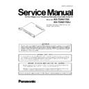
Panasonic KX-TDA6178X / KX-TDA6178XJ Service Manual ▷ View online
2
KX-TDA6178X/KX-TDA6178XJ
TABLE OF CONTENTS
PAGE
PAGE
1 Safety Precautions -----------------------------------------------3
1.1. For Service Technicians ---------------------------------3
2 Warning --------------------------------------------------------------3
2.1. About Lead Free Solder (PbF: Pb free) --------------3
3 Specifications ------------------------------------------------------4
4 General/Introduction ---------------------------------------------4
4 General/Introduction ---------------------------------------------4
4.1. General Description ---------------------------------------4
5 Technical Descriptions------------------------------------------5
5.1. Block Diagram ----------------------------------------------5
5.2. Circuit Operation -------------------------------------------6
5.2. Circuit Operation -------------------------------------------6
6 Location of Controls and Components------------------ 18
6.1. Names and Locations----------------------------------- 18
7 Installation Instructions--------------------------------------- 19
7.1. ECSLC24 Card ------------------------------------------- 19
7.2. Fastening Amphenol Connector---------------------- 21
7.3. Power Failure Connections---------------------------- 22
7.2. Fastening Amphenol Connector---------------------- 21
7.3. Power Failure Connections---------------------------- 22
8 Troubleshooting Guide---------------------------------------- 25
9 Miscellaneous ---------------------------------------------------- 32
9 Miscellaneous ---------------------------------------------------- 32
9.1. Terminal Guide of the ICs Transistors and
Diodes------------------------------------------------------- 32
9.2. How To Replace a Flat Package IC ----------------- 33
9.3. Memo-------------------------------------------------------- 34
9.3. Memo-------------------------------------------------------- 34
10 Schematic Diagram--------------------------------------------- 35
10.1. Block Diagram -------------------------------------------- 35
10.2. No.1---------------------------------------------------------- 36
10.3. No.2---------------------------------------------------------- 38
10.4. No.3---------------------------------------------------------- 40
10.5. No.4---------------------------------------------------------- 42
10.6. No.5---------------------------------------------------------- 44
10.7. No.6---------------------------------------------------------- 46
10.8. Waveform -------------------------------------------------- 47
11 Printed Circuit Board ------------------------------------------ 50
11.1. Component View ----------------------------------------- 50
11.2. Bottom View ----------------------------------------------- 51
11.2. Bottom View ----------------------------------------------- 51
12 Appendix Information of Schematic Diagram --------- 52
13 Exploded View and Replacement Parts List ----------- 53
13 Exploded View and Replacement Parts List ----------- 53
13.1. IC Data------------------------------------------------------ 53
13.2. Cabinet and Electrical Parts Location--------------- 56
13.3. Accessories and Packing Material------------------- 57
13.4. Replacement Parts List --------------------------------- 58
13.2. Cabinet and Electrical Parts Location--------------- 56
13.3. Accessories and Packing Material------------------- 57
13.4. Replacement Parts List --------------------------------- 58
3
KX-TDA6178X/KX-TDA6178XJ
1 Safety Precautions
1.1.
For Service Technicians
• Repair service shall be provided in accordance with repair technology information such as service manual so as to prevent fires,
injury or electric shock, which can be caused by improper repair work.
1. When repair services are provided, neither the products nor their parts or members shall be remodeled.
2. If a lead wire assembly is supplied as a repair part, the lead wire assembly shall be replaced.
3. FASTON terminals shall be plugged straight in and unplugged straight out.
2. If a lead wire assembly is supplied as a repair part, the lead wire assembly shall be replaced.
3. FASTON terminals shall be plugged straight in and unplugged straight out.
• ICs and LSIs are vulnerable to static electricity.
When repairing, the following precautions will help prevent recurring malfunctions.
1. Cover plastic parts boxes with aluminum foil.
2. Ground the soldering irons.
3. Use a conductive mat on worktable.
4. Do not grasp IC or LSI pins with bare fingers.
2. Ground the soldering irons.
3. Use a conductive mat on worktable.
4. Do not grasp IC or LSI pins with bare fingers.
2 Warning
2.1.
About Lead Free Solder (PbF: Pb free)
Note:
In the information below, Pb, the symbol for lead in the periodic table of elements, will refer to standard solder or solder that con-
tains lead.
We will use PbF when discussing the lead free solder used in our manufacturing process which is made from Tin, (Sn), Silver,
(Ag), and Copper, (Cu).
This model, and others like it, manufactured using lead free solder will have PbF stamped on the PCB. For service and repair
work we suggest using the same type of solder.
Caution
• PbF solder has a melting point that is 50
° ~ 70° F, (30° ~ 40°C) higher than Pb solder. Please use a soldering iron with tempera-
ture control and adjust it to 700
° ± 20° F, (370° ± 10°C).
Exercise care while using higher temperature soldering irons.:
Do not heat the PCB for too long time in order to prevent solder splash or damage to the PCB.
Do not heat the PCB for too long time in order to prevent solder splash or damage to the PCB.
• PbF solder will tend to splash if it is heated much higher than its melting point, approximately 1100
°F, (600°C).
• When applying PbF solder to double layered boards, please check the component side for excess which may flow onto the
opposite side (See figure, below).
2.1.1.
Suggested PbF Solder
There are several types of PbF solder available commercially. While this product is manufactured using Tin, Silver, and Copper,
(Sn+Ag+Cu), you can also use Tin and Copper, (Sn+Cu), or Tin, Zinc, and Bismuth, (Sn+Zn+Bi). Please check the manufac
turer's specific instructions for the melting points of their products and any precautions for using their product with other
materials.
The following lead free (PbF) solder wire sizes are recommended for service of this product: 0.3mm, 0.6mm and 1.0mm.
4
KX-TDA6178X/KX-TDA6178XJ
3 Specifications
4 General/Introduction
4.1.
General Description
This card is plugged into a free slot on the TDA600 systems and randomly connects up to 24 SLT devices.
Can only be installed in shelves in which a PSU-L is intalled.
This card sends Caller ID signal to extension ports.
The LPR is SH-1(SH7020), and the memory is composed of a 512K byte Flash ROM and a 128K byte SRAM.
It also supports a software upgrade by downloading the latest version.
Can only be installed in shelves in which a PSU-L is intalled.
This card sends Caller ID signal to extension ports.
The LPR is SH-1(SH7020), and the memory is composed of a 512K byte Flash ROM and a 128K byte SRAM.
It also supports a software upgrade by downloading the latest version.
Functional Block
Functional contents
Extension Interface
Number of Ports
24 ports
SLT Interface
-26V 26mA Feeding function
(Voltage in ports 1-8 are switched over to -45V, depending on the circuit dis-
tance.)
Dial-pulse signal detecting function
DTMF signal detecting function
Bell signal issuing function
Hook detecting function
Ringtrip detecting function
2W/4W converting function
Surge protective function
CODEC function
• Test function (Loop back, Tone generation)
• Programmable digital filtering function
• Serial interface function
• PIO function
• Programmable digital filtering function
• Serial interface function
• PIO function
DTMF Receiver
24 lines for each port
Caller ID (FSK)
24 lines for each port
On-board Ringer
20/25Hz 75Vrms
Phase control (Three-phase / Four-phase)
Phase control (Three-phase / Four-phase)
On-board DC/DC Power Supply
Input +15V
Output +3.3V
Input +40V
Output: -30V, -55V, +80V
Output +3.3V
Input +40V
Output: -30V, -55V, +80V
Power Failure Forwarding Function
4 lines supported
Self-Diagnostic Function
Carried out with outside-line interface in a pair (only one port)
Speech path test, Dial pulse test, DTMF test
Speech path test, Dial pulse test, DTMF test
ASIC
EC bus interface function
H.100 bus interface function, Digital PLL function
Local bus interface function
Time switch function, Gain controlling function, FIFO/DPRAM function
Intelligent PIO function
H.100 bus interface function, Digital PLL function
Local bus interface function
Time switch function, Gain controlling function, FIFO/DPRAM function
Intelligent PIO function
Control Unit
CPU
SH-1/SH7020 (12.288MHz)
Flash ROM
512Kbyte
SRAM
128Kbyte
FPGA
• Interface between codec and CPU
• SRAM type (XC3S250E) manufactured by XILINX
• CID128 bytes /ch transmission buffer
• SRAM type (XC3S250E) manufactured by XILINX
• CID128 bytes /ch transmission buffer
LED Display Circuit
Card status indicating LED: Two colors (Red/Green)
External Interface Connector
Extension interface
50pin Amphenol connector: 1
Power failure forwarding 4pin modular jack: 2
5
KX-TDA6178X/KX-TDA6178XJ
5 Technical Descriptions
5.1.
Block Diagram
ASIC
IC3
BB Connector
L
E
D
x 2
O
S
C
16M
O
S
C
12M
12.
288M
H
z
16.
384M
H
z
EC
CT
15V
C
a
rd_I
D
A
rea_c
o
d
e
mo
d
e
P1[
7:0]
FL
AS
H
(512KB)
IC602
SR
AM
(128KB)
IC603
PE
B
3265
IC201A
LH
W
PC
M
PFT
Re
la
y
Se
rg
e
EM
C
PFT
Jac
k
T/
R
PFT
Re
la
y
Se
rg
e
EM
C
T/
R
SCI0
CODEC I/F
FP
G
A
PFT
Se
rg
e
PFT
Jac
k
T/
R
C
O
D
E
C
2c
h
PE
B
3265
IC201C
SLI
C
2c
h
Po
rt
1
Po
rt
7,
8
PFT
Se
rg
e
T/
R
Se
rg
e
T/
R
PE
B
3265
IC201E
Se
rg
e
T/
R
SC
I1
Di
a
g
P2
6
SC
I (
7pi
n)
P2
2
,2
3
DC
/D
C
3.
3
V
VB
AT
H
VB
AT
L
VH
R
nI
N
T
nI
N
T
RING_
S
YNC
nH
A
L
T
Di
a
g
T
/R
SC
I2
CODE
C
_
n
INT
RI
N
G
_
S
Y
N
C
nH
A
L
T
Po
w
e
r Su
p
p
ly
Fo
r
Rin
g
e
r
a
n
d
T
-R V
o
lta
g
e
40
V
PE
F
4365
IC200A
PE
F
4365
IC200E
Di
a
g
Re
la
y
Di
a
g
T
/R
PF
T
P2
7
nC
S0
nC
S1
nC
S2
nC
S3
n
C
S
[3:0]
n
IRQ1
CP
U
S
H
7020
IC601
nI
R
Q
0
nI
R
Q
1
nI
R
Q
2
nI
R
Q
3
nI
R
Q
1
Po
rt
4
Po
rt
3
Po
rt
2
Po
rt
6
Po
rt
5
Po
rt
9-16
Po
rt
17-24
2.
5
V
1.
2
V
KX-TDA6178X/KX-TDA6178XJ BLOCK DIAGRAM
PE
F
4365
IC200C
IC100

