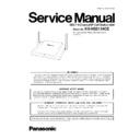
Panasonic KX-NS0154CE (serv.man2) Service Manual ▷ View online
2
KX-NS0154CE
TABLE OF CONTENTS
PAGE
PAGE
1 Safety Precautions
-----------------------------------------------3
1.1. For Service Technicians ----------------------------------3
1.2. Caution--------------------------------------------------------3
1.2. Caution--------------------------------------------------------3
2 Warning
--------------------------------------------------------------3
2.1. About Lead Free Solder (PbF: Pb free) --------------3
2.1.1. Suggested PbF Solder -------------------------------4
2.1.2. Information for Users on Collection and
2.1.2. Information for Users on Collection and
Disposal of Old Equipment and used
Batteries -------------------------------------------------4
Batteries -------------------------------------------------4
2.2. Discarding of P. C. Board --------------------------------4
3 Specifications
------------------------------------------------------5
4 Technical Descriptions
------------------------------------------6
4.1. Block Diagram ----------------------------------------------6
4.2. Main Processer ---------------------------------------------7
4.3. Power Supply Circuit -------------------------------------7
4.4. Reset circuit -------------------------------------------------7
4.5. Clock Circuit -------------------------------------------------8
4.2. Main Processer ---------------------------------------------7
4.3. Power Supply Circuit -------------------------------------7
4.4. Reset circuit -------------------------------------------------7
4.5. Clock Circuit -------------------------------------------------8
4.5.1. System Clock ------------------------------------------8
4.5.2. PLLIC-----------------------------------------------------8
4.5.2. PLLIC-----------------------------------------------------8
4.6. Memory Access Circuit -----------------------------------8
4.6.1. IC100 -----------------------------------------------------8
4.6.2. IC501 and IC503 --------------------------------------8
4.6.2. IC501 and IC503 --------------------------------------8
4.7. Ethernet Circuit ---------------------------------------------8
4.8. RF Circuit-----------------------------------------------------9
4.9. LED Circuit---------------------------------------------------9
4.8. RF Circuit-----------------------------------------------------9
4.9. LED Circuit---------------------------------------------------9
5 Location of Controls and Components
------------------ 10
5.1. Names and Locations----------------------------------- 10
6 Installation Instructions
--------------------------------------- 10
7 Firmware update
------------------------------------------------ 11
7.1. Firmware update ----------------------------------------- 11
8 Service Mode
----------------------------------------------------- 12
8.1. How to Change MAC Address Label---------------- 12
8.1.1. Replacing Main P.C.B. ----------------------------- 12
8.1.2. Attaching MAC Address Label ------------------- 12
8.1.2. Attaching MAC Address Label ------------------- 12
9 Troubleshooting Guide
---------------------------------------- 13
9.1. No Power--------------------------------------------------- 13
9.2. No Operation ---------------------------------------------- 14
9.3. System Check--------------------------------------------- 17
9.2. No Operation ---------------------------------------------- 14
9.3. System Check--------------------------------------------- 17
10 Disassembly and Assembly Instructions
--------------- 18
10.1. Disassembly Instructions------------------------------- 18
11 Measurements and Adjustments
-------------------------- 19
11.1. USB Test Mode ------------------------------------------- 19
11.1.1. How to Install the Application for Test
Mode---------------------------------------------------- 19
11.2. Clock Adjustment----------------------------------------- 22
12 Miscellaneous
---------------------------------------------------- 23
12.1. Terminal guide of ICs, Transistors and Diodes --- 23
12.2. How To Replace a Flat Package IC ----------------- 24
12.2. How To Replace a Flat Package IC ----------------- 24
12.2.1. Preparation-------------------------------------------- 24
12.2.2. Removal Procedure--------------------------------- 24
12.2.3. Procedure --------------------------------------------- 24
12.2.4. Removing Solder From Between Pins --------- 24
12.2.2. Removal Procedure--------------------------------- 24
12.2.3. Procedure --------------------------------------------- 24
12.2.4. Removing Solder From Between Pins --------- 24
12.3. How to Replace the LLP (Leadless Leadframe
Package) IC and IC ground plate -------------------- 25
12.3.1. Preparation-------------------------------------------- 25
12.3.2. Caution------------------------------------------------- 25
12.3.3. How to Remove the IC ----------------------------- 25
12.3.4. How to Install the IC -------------------------------- 25
12.3.2. Caution------------------------------------------------- 25
12.3.3. How to Remove the IC ----------------------------- 25
12.3.4. How to Install the IC -------------------------------- 25
12.3.5. How to Remove a Solder Bridge (Doesn't
apply to IC ground plate.) ------------------------- 26
13 Schematic Diagram
-------------------------------------------- 27
13.1. Main Board ------------------------------------------------ 27
13.1.1. No.1 ---------------------------------------------------- 27
13.1.2. No.2 ---------------------------------------------------- 28
13.1.3. No.3 ---------------------------------------------------- 29
13.1.4. No.4 ---------------------------------------------------- 30
13.1.5. No.5 ---------------------------------------------------- 31
13.1.2. No.2 ---------------------------------------------------- 28
13.1.3. No.3 ---------------------------------------------------- 29
13.1.4. No.4 ---------------------------------------------------- 30
13.1.5. No.5 ---------------------------------------------------- 31
13.2. Waveform-------------------------------------------------- 32
13.2.1. No.(1)-(7)---------------------------------------------- 32
13.2.2. No.(8)-(15) -------------------------------------------- 33
13.2.3. No. (16)-(18) ----------------------------------------- 34
13.2.2. No.(8)-(15) -------------------------------------------- 33
13.2.3. No. (16)-(18) ----------------------------------------- 34
14 Printed Circuit Board
------------------------------------------ 35
14.1. Component View----------------------------------------- 35
14.2. Bottom View----------------------------------------------- 36
14.2. Bottom View----------------------------------------------- 36
15 Appendix Information of Schematic Diagram
-------- 37
16 Exploded View and Replacement Parts List
----------- 38
16.1. IC Data ----------------------------------------------------- 38
16.1.1. IC100 (DVF99) -------------------------------------- 38
16.1.2. IC101 (DDR2)---------------------------------------- 44
16.1.3. IC102 (NAND Flash Memory) ------------------- 46
16.1.4. IC302 (PHY)------------------------------------------ 47
16.1.5. IC501 (DCX81 (RF & DSP)) --------------------- 48
16.1.6. IC502 (Serial Flash Memory) -------------------- 50
16.1.7. IC503 (DCX81 (DSP)) ----------------------------- 51
16.1.8. IC504 (Serial Flas Memory) ---------------------- 53
16.2. Cabinet and Electrical Parts Location -------------- 54
16.3. Accessories and Packing Material ------------------ 55
16.4. Replacement Parts List -------------------------------- 56
16.3. Accessories and Packing Material ------------------ 55
16.4. Replacement Parts List -------------------------------- 56
16.4.1. Cabinet and Electrical Parts---------------------- 56
16.4.2. Accessory and Packing Materials -------------- 56
16.4.3. Main Boards Parts ---------------------------------- 56
16.4.4. FIXTURES AND TOOLS-------------------------- 60
16.4.2. Accessory and Packing Materials -------------- 56
16.4.3. Main Boards Parts ---------------------------------- 56
16.4.4. FIXTURES AND TOOLS-------------------------- 60
17 Appendix
---------------------------------------------------------- 61
3
KX-NS0154CE
1 Safety Precautions
1. Before servicing, unplug the AC power cord to prevent an electric shock.
2. When replacing parts, use only the manufacturer's recommended components.
3. Check the condition of the power cord. Replace if wear or damage is evident.
4. After servicing, be sure to restore the lead dress, insulation barriers, insulation papers, shields, etc.
5. Before returning the serviced equipment to the customer, be sure to perform the following insulation resistance test to prevent
the customer from being exposed to shock hazards.
1.1.
For Service Technicians
• Repair service shall be provided in accordance with repair technology information such as service manual so as to pre-
vent fires, injury or electric shock, which can be caused by improper repair work
.
1. When repair services are provided, neither the products nor their parts or members shall be remodeled.
2. If a lead wire assembly is supplied as a repair part, the lead wire assembly shall be replaced.
3. FASTON terminals shall be plugged straight in and unplugged straight out.
2. If a lead wire assembly is supplied as a repair part, the lead wire assembly shall be replaced.
3. FASTON terminals shall be plugged straight in and unplugged straight out.
• ICs and LSIs are vulnerable to static electricity.
When repairing, the following precautions will help prevent recurring malfunctions.
1. Cover plastic parts boxes with aluminum foil.
2. Ground the soldering irons.
3. Use a conductive mat on worktable.
4. Do not grasp IC or LSI pins with bare fingers.
2. Ground the soldering irons.
3. Use a conductive mat on worktable.
4. Do not grasp IC or LSI pins with bare fingers.
1.2.
Caution
When you note the serial number, write down all of the 11 digits.
The serial number may be found on the label affixed to the bottom of the unit.
The serial number may be found on the label affixed to the bottom of the unit.
2 Warning
2.1.
About Lead Free Solder (PbF: Pb free)
Note:
In the information below, Pb, the symbol for lead in the periodic table of elements, will refer to standard solder or solder that con-
tains lead.
We will use PbF when discussing the lead free solder used in our manufacturing process which is made from Tin, (Sn), Silver,
(Ag), and Copper, (Cu).
This model, and others like it, manufactured using lead free solder will have PbF stamped on the PCB. For service and repair
work we suggest using the same type of solder.
Caution
• PbF solder has a melting point that is 50 ~ 70 F, (30 ~ 40C) higher than Pb solder. Please use a soldering iron with tempera-
ture control and adjust it to 700 ± 20 F, (370 ± 10C).
Exercise care while using higher temperature soldering irons.:
Do not heat the PCB for too long time in order to prevent solder splash or damage to the PCB.
Exercise care while using higher temperature soldering irons.:
Do not heat the PCB for too long time in order to prevent solder splash or damage to the PCB.
• PbF solder will tend to splash if it is heated much higher than its melting point, approximately 1100F, (600C).
• When applying PbF solder to double layered boards, please check the component side for excess which may flow onto the
• When applying PbF solder to double layered boards, please check the component side for excess which may flow onto the
opposite side (See figure, below).
4
KX-NS0154CE
2.1.1.
Suggested PbF Solder
There are several types of PbF solder available commercially. While this product is manufactured using Tin, Silver, and Copper,
(Sn+Ag+Cu), you can also use Tin and Copper, (Sn+Cu), or Tin, Zinc, and Bismuth, (Sn+Zn+Bi). Please check the manufac
turer's specific instructions for the melting points of their products and any precautions for using their product with other
materials.
The following lead free (PbF) solder wire sizes are recommended for service of this product: 0.3mm, 0.6mm and 1.0mm.
2.1.2.
Information for Users on Collection and Disposal of Old Equipment and used Bat-
teries
teries
2.2.
Discarding of P. C. Board
When discarding P. C. Board, delete all personal information such as telephone directory and caller list or scrap P. C. Board.
5
KX-NS0154CE
3 Specifications
IP-CS Specification
RF Specification
CAUTION
• The IP-CS should be kept free of dust, moisture, high temperature (more than 40 C), low temperature (less than 0 C), and
vibration, and should not be exposed to direct sunlight.
• The IP-CS should not be placed outdoors (use indoors).
• The IP-CS should not be placed near high-voltage equipment.
• The IP-CS should not be placed on a metal object.
• The IP-CS should not be placed near high-voltage equipment.
• The IP-CS should not be placed on a metal object.
Items
Description
Type
4 channel CS
Supported Audio
Narrowband
Radio Method
DECT
VoIP Signalling Protocol
MGCP
IP Port Number Flexible Setting
Yes
Local Setting
Yes (through Web application)
Site Survey Mode
Yes (through Web application)
Initialisation
Yes (through Web application)
Maximum Simultaneous Calls
4 (8 with Activation key)
Power Supply
PoE
(IEEE 802.3af)
Optional AC adaptor
(KX-A239CE [PQLV206CE]/KX-A239UK [PQLV206E]/
KX-A239BX [PQLV206CE]/KX-A239EJ [PQLV206E]/
KX-A239AL [PQLV206AL])
VoIP Audio Codec
G.711, G.729A, G.726
LAN Port
10 BASE-T
100 BASE-TX
VLAN
Yes (802.1Q)
IP Addressing
DHCP
Static IP Address Setting
Software Upgrade
Yes
Built-in VPN
No
Weight
290 g
Size
(W) 190 mm x (H) 133.9 mm x (D) 39.3 mm
Items
Description
Radio Access Method
MultiCarrier TDMA-TDD
Frequency Band
1880 MHz to 1900 MHz
Number of Carriers
10
Carrier Spacing
1728 kHz
Transmission Output
Peak 250 mW


